
Protec MEMS Technology orders maskless lithography system from EV Group
PROTEC MEMS Technology (PMT), a leading supplier of semiconductor wafer probe cards, has ordered a LITHOSCALE maskless exposure system from EV Group (EVG), a leading supplier of wafer bonding and lithography equipment for the MEMS, nanotechnology and semiconductor markets. The LITHOSCALE system will be installed at PMT’s headquarters in Asan-si, Chungcheongnam-Do, South Korea, where it will be used in the production of next-generation MEMS-based probe cards for wafer-level testing of advanced NAND, DRAM and High Bandwidth Memory (HBM) devices.
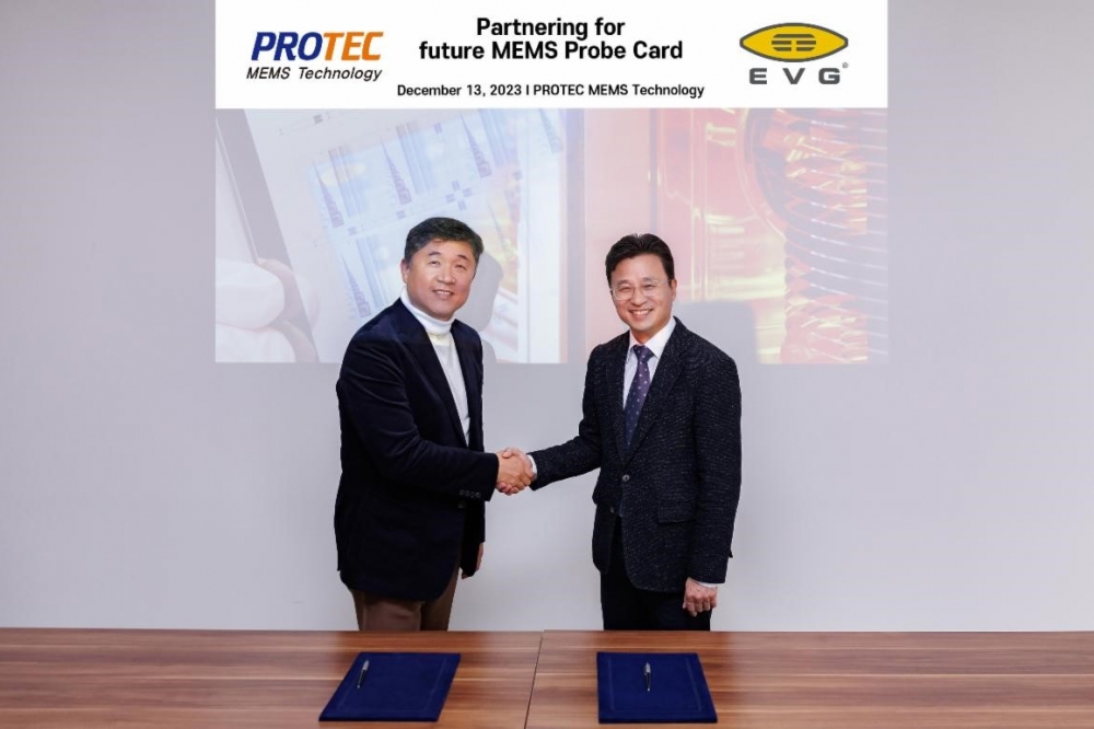
PROTEC MEMS Technology (PMT) and EV Group sign agreement on maskless lithography for advanced wafer memory probe card manufacturing. Shown here from left to right are Mr. Yong-Ho Cho, CEO of PMT, and
Mr. Young-Sik Yun, general manager of EV Group Korea.
“Fine-pitch probe card manufacturing involves many lithographic patterning steps, which can significantly drive up cost of ownership,” stated Dr. Yong-Ho Cho, CEO of PMT. “We can achieve significant cost savings, faster process development, and improved process performance, by switching from traditional lithography to EV Group’s LITHOSCALE maskless exposure product. We look forward to future collaborations with EVG leveraging LITHOSCALE and other process solutions for advanced probe card manufacturing.”
Incorporating EVG’s MLE™ (maskless exposure) technology, LITHOSCALE addresses lithography needs for markets and applications that require a high degree of flexibility or product variation. LITHOSCALE tackles legacy bottlenecks by combining powerful digital processing that enables real-time data transfer and immediate exposure, high structuring resolution and throughput scalability. It is ideally suited for rapid prototyping, providing fast turnaround and R&D cycle times.
MEMS manufacturing in particular poses challenges for lithography due to its complex product mixes, which drive up mask overhead costs. LITHOSCALE’s mask-free approach eliminates mask-related consumables, addressing the demand for low-cost-of-ownership patterning in wafer probe card manufacturing. In addition, LITHOSCALE’s high depth of focus and high resolution (sub-2-micron L/S) enables maskless patterning of dense redistribution layer (RDL) and via connections, which supports technology scaling for fine-pitch probe cards.
According to Young-Sik Yun, general manager of EV Group Korea, “Wafer-level testing with probe cards is an essential process for improving device production yields and reducing overall test cost per die. LITHOSCALE offers a unique combination of high resolution, high flexibility to handle many different product designs, and low cost of ownership, making it an ideal solution for manufacturing fine-pitch wafer probe cards. We are pleased to support PMT in their efforts to expand their product portfolio and shorten their development cycles.”


