Superconductors on silicon 'breakthrough'

Ambature has announced success in growing its high-temperature superconducting material (a-axis YBCO) on silicon in its labs in Waterloo, Ontario.
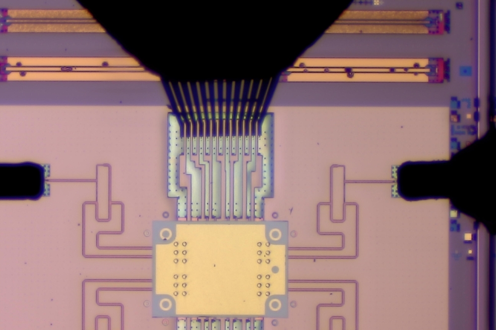
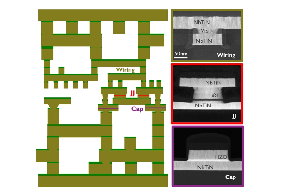
This uniquely oriented YBCO enables simpler fabrication of Josephson junctions—superconducting counterparts to transistors—in semiconductor foundries. In turn, these Josephson junctions can be used to build sensors and extremely fast and energy-efficient high-performance computers needed for advanced applications.
"The recent high-quality growth of our material on silicon opens up the semiconductor industry to Ambature. Our superconducting sensors and computer processors can be fabricated at scale using existing equipment in semiconductor foundries" said Mitch Robson, Ambature Lead Scientist.
The semiconductor industry is searching for new materials and architectures to overcome limitations of existing CMOS technology. The New York Times reported that Ivan Sutherland, one of the pioneers of CMOS, believes superconducting digital circuits may be the next great opportunity: "The nation that best seizes the superconducting digital circuit opportunity will enjoy computing superiority for decades to come." Among superconducting materials, low-temperature superconductors have high cooling overheads that largely confine their use to quantum computing applications. Scalable a-axis high-temperature superconductors are better candidates for applications like data centers because cooling them is much easier. "This leap forward allows us to accelerate our plans to commercially scale our technology and become the bridge between semiconductor and superconductor electronics" said Ron Kelly, Ambature CEO.
Superconducting materials and circuits offer intrinsic benefits to telecommunications, medical diagnostics, autonomous vehicles, IoT, data centers and AI. These applications have multiple use cases in both commercial and military markets. Integrating with silicon, often referred to as "CMOS+X," is an increasingly prevalent strategy to harness the beneficial properties of new materials while taking advantage of the mature silicon manufacturing capabilities of the semiconductor industry. With two means of successfully integrating with silicon—heterogeneously via thermocompression bonding for chiplets and now epitaxially via silicon substrates with buffer layers—Ambature is well poised to support its licensees as they develop the world's most advanced sensors and computers.


