
Accelerating mechanical stress simulation for 3D-IC reliability in the cloud
Marc Swinnen, Product Marketing Director at Ansys, discusses recent
collaboration with TSMC and Microsoft to develop a joint solution which
provides a high-capacity cloud solution for analysing the mechanical
stresses in 2.5D/3D- IC multi-die systems, which lets joint customers
avoid field failures and extends product lifetime and reliability.
PHILIP ALSOP, EDITOR asks the questions.
PA: Ansys has been collaborating with TSMC and Microsoft, focusing on analysing mechanical stresses in multi-die 3D integrated circuit systems.The obvious place to start would be to understand how did the collaboration come about?
MS: Our collaboration with TSMC has been going on for decades. That’s based largely on the fact that Ansys sells and produces the RedHawk-SC™ product, which is an electronic design automation (EDA) software tool used by chip designers to verify the power integrity of their chip. Basically, every chip has a power and ground network on it. Every single transistor has to be connected to power and has to be connected to ground, like any electronic device. If you have 50 billion transistors on your chip, that means you must design two electric networks, each with 50 billion endpoints. So, these are incredibly large and complicated on-chip networks that are vital to the proper functioning of the chip. They need to be checked because there is always voltage drop on the power lines. And these days, to save power, the voltage is so low that you really can’t afford to lose even 100 millivolts going from the package pin to the actual transistor. Hence everything has to be very carefully analysed to make sure your power integrity, or voltage drop, is properly accounted for and will meet your spec.
And that’s a very big, tough problem. And that’s what RedHawk-SC does. It does the final sign off for manufacturing, saying, yes, this will work. Of course, this all relies critically on the manufacturing rules. We work very closely with all of the major foundries, including TSMC. TSMC and Ansys have a longstanding collaborative association to get this golden sign off tool out to the industry - the large majority of all the chips in the world are signed off for their power integrity using Ansys Redhawk-SC. That is the foundation of our deep and ongoing collaboration with TSMC.

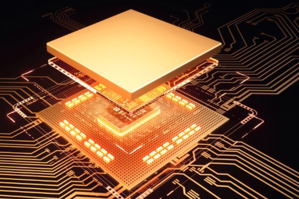
Which brings us to the topic under discussion. Traditionally, a chip, or integrated circuit (IC), is a monolithic piece of silicon - it’s all one thing. You cut it out of the wafer and it’s one little chip of silicon which gets embedded in a package. But now, for multiple reasons, it is no longer possible to build the big systems you want today on just a sing chip. So, they’ve started making multiple chips and putting them together into a system we call 3D IC - where you stack several chips on top of each other or, more commonly, you put them right next to each other, which we call two-and-a-half D. I’ll just call all of these configurations 3DIC - all these different ways of stacking or putting them right next to each other. The idea of a 3DIC is that it contains multiple dice. So bare dice, not packaged dice, that are placed right next to each other. Usually they’re placed on top of another chip, called an interposer, which connects them all together. All high-performance computing is going there today.
Now, some of these dice get hot and some of them get less hot and so you have differential thermal expansion. The dice are connected to each other with micro bumps. These are tiny, tiny bumps - up to a thousand per square millimetre - and they can’t stand very much shear stress. If your assembly starts expanding and contracting differentially and cycling through these thermal cycles, you’re going to get mechanical deformation, warping and stresses in this 3D assembly. And that is something radically new for chip designers. I mean, someone always had to worry about thermal expansion at some point. Usually a system or package designer way down the line, after the chip was assembled on a board and the board was put in the system and the system was in the heatsink - at that point, somebody did some mechanical analysis. But now it’s come crashing down onto the chip, designers now have to worry right out of the gate, how is this thing going to deform and warp? And if I use the wrong materials or use the wrong floor plan, my design will have much lower reliability than if it’s done properly. Hence, they need to do mechanical simulations early on, and predict thermo mechanical behaviour.
Ansys has a rich history in this area - beyond the semiconductor division we have many other simulation tools. We have computational fluid dynamics, we have mechanical, we have safety, we have optics, we have electromagnetics - many, many fields. But mechanical is one of our specialties where we are industry leading. It was natural for us to take those algorithms and apply them to our semiconductor problem.

TSMC worked with us to solve some of the issues they’ve seen in their own production and design side of things. They saw this as a problem which they needed solving. It’s a tough computational problem so they pulled in Microsoft Azure to give the cloud computing capabilities required to really solve this in the required timeframe. With cloud computing from Microsoft, the mechanical/thermal simulation from Ansys, and the manufacturing capability from TSMC, together we came up with a solution flow that worked and has been proven to work.
PA: And the objective of the project, I believe it’s to provide added confidence to address novel multi-physics requirements that improve the functional reliability and increase product lifetimes of advanced 3D fabric designs?
MS: So, there’s two points to that. One is novel, and the other one’s reliability. So why is this novel? Mechanical simulation is not novel in itself, but for semiconductor designers, it is. As I already mentioned, this was something monolithic designers never had to worry about. But 3D assemblies - and I use 3D as a catch-all name for all those different architectures that the foundries supply with chip-on-chip and chip-next-to-chip - there’s lots of ways of arranging these chips. I’ll just call them all 3D-IC
So that is novel for chip designers that they now have to think at the floor planning stage: Okay, which of these chips is going to get hot, which is going to stay cooler? If I put two hot chips right next to each other, is that going to be a thermal problem that I can’t fix? Or especially if two chips get hot in the same activity mode, like in streaming mode while you’re playing video, both these chips get really hot in this corner. That could doom my project right from the get go.
Thermal is the number-one limitation on achievable integration density today. You can very easily stack chips several layers deep. You can design that. You can manufacture that. All that is not a problem. The problem is you can’t cool it! It’ll get too hot, and it’ll melt. So how close and how compact you can make a system is determined, number one, far and away, by power dissipation. How do I control and manage my heat dissipation? So, when you’re assembling these large systems, multiple chips together - and we’re talking up to a dozen chips - how do I manage my power?

With heat comes thermal expansion, temperature cycling, and differential expansion of multiple materials. Monolithic chips are made out of one thing, silicon. Now suddenly you have systems that may include silicon chips together with silicon carbide chips and organic substrates. The individual chips are usually placed on an interconnection substrate called an interposer. The interposer is often made of silicon, like a giant chip made with an old process, like 35 nanometre or something.
But interposers can be made of organic resin as well. It can also be glass. There are foundries working with glass substrates. So, there’s multiple materials in this stack-up and they all expand differentially. This mechanical concern is novel to most chip designers today. They may have expertise in the company somewhere that deals with thermal issues in electronic systems, but it’s not in the chip design group. As a result, they may have to reorganise how the company is set up so that this mechanical expert is involved right from the get go. So that’s novel to them.
Ansys is taking our multiphysics simulation capabilities and making them available in a way that works with semiconductor data formats in a semiconductor flow. That is what we believe to be the answer. We have a tool called RedHawk-SC Electrothermal™, which takes care of integrating these. On the reliability side, the fundamental benefit is that thermal expansion is something that will, over time, degrade the chip. As I said, these chips are connected through little solder bumps that connect when you press the chips together.
They’re about 10 micrometres apart, which gives you a very high density of interconnect. But if these chips start bending, warping or twisting and you get shear stresses between them, it’s very easy for these micro bumps to shear, to break or to deform slightly so that their contact point becomes diminished. Which means that the power density or current density through that bump becomes higher and the chance of them melting becomes higher.
We did a 3D-IC assembly recently, with 400,000 micro bumps in the system, and you can have millions of micro bumps. If any one of them fails, you could have a system failure. It really behoves you to very carefully consider how your multi-die system warps as it heats up and cools down over time. That will give you a reliability problem if not properly managed.

Chips have very specific rules about tolerance to bending. For example, a chip, is allowed to bend to a certain amount in the concave way - only so much. And by the way, it’s not only heating that causes it to bend, but also during assembly, when they’re actually mounting these chips on top of each other, you press the chips down and that bends them a little bit. So that needs to be taken into account, too. Concave bending is allowed to a certain degree, but convex bending is absolutely not allowed.Apparently, there’s very low tolerances on that. One way of bending is allowed, the other one isn’t. These are some of the reliability issues that come up and there’s trade-offs to be made there.
PA: If I understand you correctly, the issue is, because this is a completely novel process, there needs to be a lot of learning to take place. Once they have understood how all you’ve described happens, they will then find out the optimum way to make these 3D systems. But until they do, they have to carry out multiple tests under all different loads and conditions. And if they do things in exactly the same way each time, they will get the same results? Or are there variations, what we might call random variations, even in identical conditions?
MS: Yes, that is the beauty of simulation. People might say, I prefer working on a real system that doesn’t predict what it’s going to do, but actually you can measure on the test bench. Yes, there’s a benefit to measuring reality, but the problem is you’re measuring a specific instance of reality. You’re measuring this particular device with this particular set of parameters. As an example, imagine measuring the parameters of something like steel bolts. How strong is a steel bolt? Well, some will be a little stronger than others. Batches of steel vary. There’s a range there. You can test a particular bolt and that might be a strong one or it might be a weak one, but it doesn’t tell you what the range of possibilities are when I’m going to build thousands of these things into a bridge. So too, when you take a chip under test or 3D assembly, you can put it on the test bench and test it, but you’re testing a particular device. But there’s so many different parameters in thickness variation, material property variation. Also temperature or thermal is due to activity, right? If the chip isn’t doing anything, it doesn’t get hot, it’s only when it’s actually active that it starts to get hot.
So what activity are you going to give it? And that’s a problem because there’s many, many thousands, millions of possible activity combinations. Simulation allows you to test across a variety of parameters, a variety of conditions, a variety of environmental, ambient conditions, too, and do all this with a variety of material combinations and verify that the system will work across this entire envelope of possibilities. That’s the power of simulation in general. That is what RedHawk SC Electrothermal allows you to do as well. You can identify problems and then decide what you’re going to do about fixing these or how to prevent them. One of the trade-offs you have to consider is this silicon interposer. It’s much bigger than a standard chip, we’re talking three inches by three inches or so. This interposer, if you make it thick, then it will not warp as much. It’ll be stiffer, it won’t deform as much, which is good, but that means that you get much higher thermal stresses. The differential expansion wants to be there but it can’t bend, so the stresses will be very high, but it won’t deform as much. But if you make the interposer much thinner, it’ll deform much more, but the stresses will be lower. Like everything in engineering, it’s a trade-off.

Also, there are holes drilled through that punch through the silicon interposers to connect from one side to the other. These holes are called through- silicon vias (TSVs) and they’re typically copper pillars. They’re tiny, but for a chip size they are actually quite big. Even though they’re electrical conductors meant to connect signal wires, they also serve a good purpose of dissipating the heat down through the silicon. There are different ways you can arrange these, not just for the electrical functionality, but also for the heat functionality. This is another way in which you can even-out the heat to reduce the amount of differential expansion, which will reduce the stresses. Getting an optimal pattern of TSVs is another way you could optimise your design. There are a lot of angles to look at to see if the design can be improved.
PA: What you’re describing, the main challenge is scaling up what you might call computationally demanding stress simulations, but crucially, at the same time, maintaining the predictive accuracy alongside. How big is that challenge?
MS: These thermal simulations can be very accurate and rely on meshing. You break the design down into a finite element mesh, which means you break down the whole pattern into millions of tiny little triangles that model the design geometry and can be analysed as a small local problem. A fine mesh gives you high accuracy but takes a long time to solve. And we’re talking days to weeks of computation on hundreds of CPUs, and so that can become prohibitively expensive.
There are two ways to address the huge computational demands of these simulations. One is to improve your algorithms, and that’s Ansys’s job. We have things like adaptive meshing, to check if the mesh really needs to be that fine everywhere. Some places have a lot of thermal gradient, and yes, I have to model that with a fine mesh to capture those curves. But a lot of the chip, the cooler parts, have a pretty even temperature across them. I don’t need a fine mesh to model that. I can do a much faster, coarser mesh and still get accurate results. So, you have adaptive meshing which is fine, where it needs to be, and it can be coarser where it doesn’t need to be, and that really brings the computation time down. That’s the algorithmic side.
But the other side is, no matter what you do, it’s still a big tough problem. So that’s where we pull in people like Microsoft and cloud providers to say, okay, we need to routinely allow for big compute times for big 3DICs. Routinely, these systems are simulated and analysed on the cloud. And that can be a mixed on-prem or off-prem cloud, or completely on the commercial cloud. But we work with the cloud vendors like Microsoft to ensure that the Ansys product works easily on the cloud, that these algorithms are distributed efficiently, but also things like resiliency. What if one of the CPUs goes down? Can the whole job recover from a single failure and not lose two days of simulation time because one CPU went down? Also, can we use the cloud spot market? It’s a lot cheaper than using on-demand resources.
There are a lot of issues to deal with in making sure this all works in the cloud. And that was the reason why Microsoft was involved in this particular collaboration with TSMC. Microsoft makes its own chips too, so it’s sort of mutual relationship. We work with them as a customer, we work with them as a cloud vendor. It all works together. So yes, they make sure that these computationally very demanding jobs can be done within eight hours or so - if you throw several hundred or several thousand CPUs at it. We’ve run RedHawk-SC at one customer on up to 4000 CPUs to get a detailed, full- system simulation result.

PA: The 3D chip as a concept is relatively new and requires a new manufacturing process. Hence TSMC’s need to understand much of what you have outlined in terms of 3D chip design and subsequent performance?
MS: Yes, multi-die assembly is not something TSMC, being a chip manufacturing operation, had to worry too much about this in the past, especially since they’re not system designers and don’t do board assemblies. They just worry about the monolithic chip. Mechanics wasn’t really an issue. However, now they have developed 3D architectures and technologies. TSMC has a reputation of making sure that their manufacturing is not just accurate manufacturing, but also that flows are available for their customers to be able to design these things. So, their concern goes beyond just manufacturing, but also can this fit in a flow that customers can take advantage of? They’re very proactive in that sense. And they work with developing these reference flows for customers so that customers know what tools to use and how to use them to come to a good result that TSMC has validated against silicon and in the lab. So, for TSMC, mechanical simulation was a novel sort of thing to worry about. Most customer design teams still haven’t grappled with mechanical deformation,. It is only the very leading edge that has dealt with this.
If you look at who has adopted 3D-IC today, it’s the really the big HPC providers, the high end of the semiconductor design community. Nvidia, AMD, Intel, IBM, ST, those are the companies that have the volume and the density system requirements to go for full 3D. But it’s starting to trickle down more to the mainstream. Since there are so many options for building a 3DIC, the foundries have stepped up and said, okay, we will propose a number of architectures that you could use, and that are supported by our manufacturing and that we’ve shown work reliably. This is something new. Typically, the foundries have stayed a little away from packaging. It was done by a different set of industries called OSAT (outsourced system assembly and test). And the foundries focused on making the die, which then went off for packaging.
With 3D, it’s not clear where the die ends and the package starts and so the foundries have stepped up and said, okay, we’ve proposed these architectures, and you can go on their websites and find these. There are multiple architectures with reference flows to validate them. So that’s pulled foundries into something like mechanical simulation, because that’s what their customers will have to do and it’s on their architecture, with their manufacturing. They feel a responsibility to verify this all works.
PA: The importance of what you’re providing to them, from what you described, has ramped up several notches because they’re now underpinning these architectures, as opposed to potentially handing off some of the problem in a different direction as they might have done previously?
MS: Yes, exactly. 3D-IC is an emerging market that’s very much still in flux. Like I say, there’s many, many architectures which indicates that there’s no settled agreement on which is the best way of doing it. There’s still lots of technologies being tried. When you look at a 3D chip, you can look at it from two perspectives. You can say this is just a PCB but sort of shrunk down like a very high-density PCB. Or you can look at it from the other side and say no, it’s like a chip but only bigger and more expanded. And customers have approached it from both sides. Some have a more PCB background, some have a more a chip background. Is it as a small PCB orbig chip? It’s somewhere in the middle and it sort of collapses all those problems into a single ball of wax, which is the seat of the problem. What I’ve seen is that, while both approaches are still used by customers, the foundries have stepped up their efforts to the point where I think this is becoming much more a silicon-oriented problem and I think in the future it’ll be designed more like a giant chip.
Both perspectives have issues: If you look at it from the chip side, these interposer layers and the connections between the chips are very PCB-like. They have river routing, there are redistribution layers that are not Manhattan. You have through- silicon vias which are very large. Chip tools are not comfortable with all this PCB variability. PCB tools can handle all that. The problem is PCB tools can’t handle the scale and the capacity of these systems. So, they’re used to running a few thousand signals, but on an interposeryou can have millions of signals and the PCB tools just don’t have the capacity to handle these millions of signals. So, both sides have issues and have toup their game and so new tools are coming on the market to handle that. For example, Synopsys has a product called 3DIC Compiler™, which is derived from their chip tools, but intended specifically for 3DIC.
PA: In terms of where you are with TSMC, I believe the solution has been validated?
MS: TSMC does have reference flows for their customers. So they can say, hey, here’s a validated flow that we’ve been able to run through, and we know this works. But they also have their own backroom operations where they design their own IPs and some chips. This particular collaboration originated more from TSMC’s own internal needs. It was more their own production people saying, “Hey, we see this as a problem”. They collaborated with us on this flow and have also published an application note on how this all works. It’s available on the TSMC design portal for all TSMC customers to access. So, it is very much a practical user perspective as opposed to simply a reference flow for the foundry.


