UK chips funding boost

Two new ‘Innovation and Knowledge Centres’ will receive £11m each to help bring new chip technologies to market.
New funding and support has been unveiled to back British scientists working on chip development which could help to power advancements in AI and will underpin the technologies needed to reach net zero.
To coincide with the Department for Science, Innovation and Technology’s one-year anniversary – two new research hubs in Southampton and Bristol have received a cash injection to boost research in silicon photonics and compound semiconductors.
Visiting the Southampton centre, Minister for Tech and the Digital Economy Saqib Bhatti said: "This investment marks a crucial step in advancing our ambitions for the semiconductor industry, with these centres helping bring new technologies to market in areas like net zero and AI, rooting them right here in the UK.
“Just nine months into delivering on the National Semiconductor Strategy, we’re already making rapid progress towards our goals. This isn’t just about fostering growth and creating high-skilled jobs, it's about positioning the UK as a hub of global innovation, setting the stage for breakthroughs that have worldwide impact.”
Each £11 million site will help convert scientific findings into business realities. They will support promising research and projects, offering researchers access to state-of-the-art prototyping technology essential for testing their complex designs, and nurturing early-stage companies. This includes empowering spin-outs with training, workshops, and vital industry contacts, ensuring they are fully equipped for when their products are market-ready.
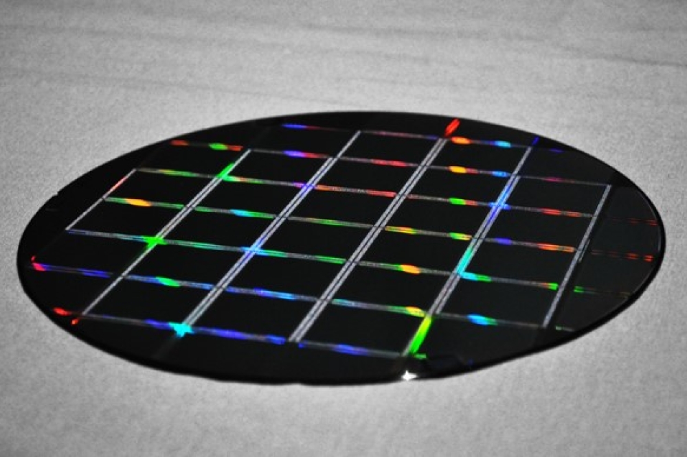
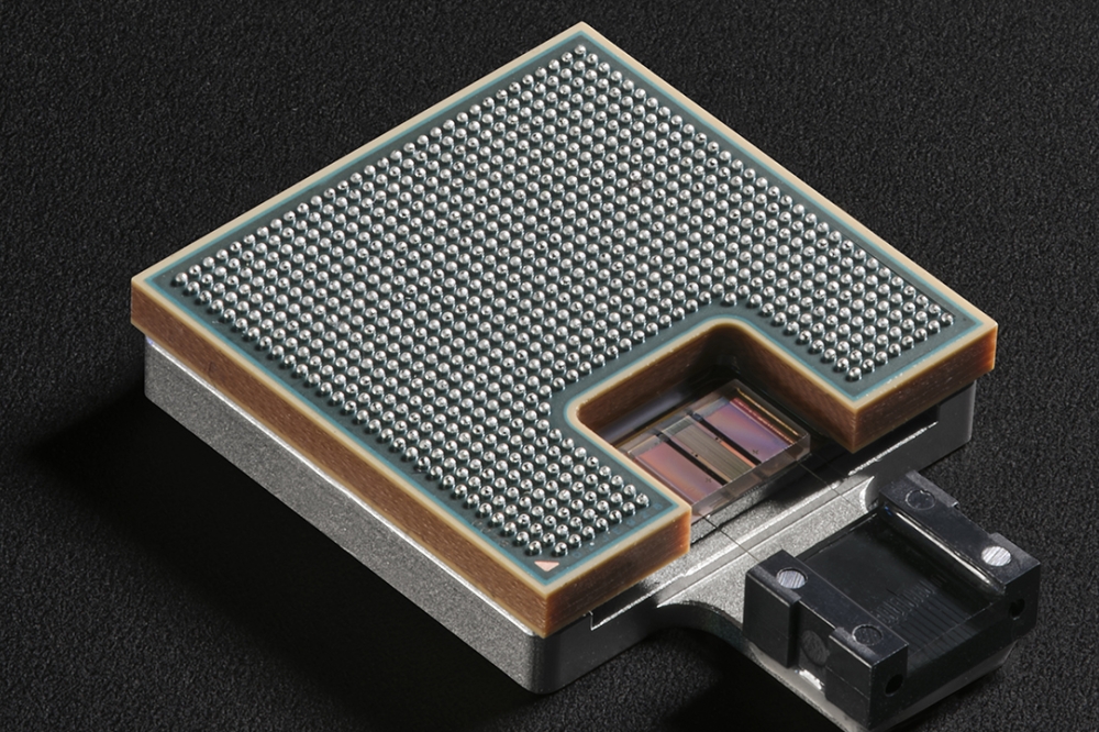
The “Cornerstone” Information and Knowledge Centre in Southampton will build on the University’s specialism in silicon photonics. This is an emerging area of research in semiconductors, where light is used to communicate information instead of electricity – meaning the chips that are made using this technology are much, much quicker than standard semiconductors.
World-leading silicon photonics researcher Professor Graham Reed, who will lead the Cornerstone facility, said: “The CORNERSTONE IKC will unite leading UK entrepreneurs and researchers, together with a network of support to improve the commercialisation of semiconductors and deliver a step-change in the silicon photonics industry.”
A further funding of £4.8 million in 11 semiconductor skills projects nationwide aims to elevate talent across all educational tiers, from school through to university and beyond. This funding will not only raise awareness of the semiconductor industry but also help to address key gaps in the UK's workforce talent and training framework.
The centres will help to deliver on the ambitions of the government’s £1bn National Semiconductor Strategy, a 20-year plan detailing how the government will drive forward the UK’s strengths and skills in design, R&D and compound semiconductors.


