
Toppan Photomask signs agreement with IBM
Advancing development of EUV photomasks for IBM’s 2 nanometer technology designs.
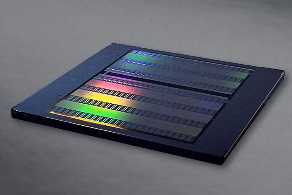
Toppan Photomask has entered into a joint research and development agreement with IBM related to the 2 nanometer (nm) logic semiconductor node, using extreme ultraviolet (EUV) lithography. This agreement also includes High-NA EUV photomask development capability on next-generation semiconductors.
Based on this agreement, for a period of five years starting 1Q 2024, IBM and Toppan Photomask plan to develop photomask capability at the Albany NanoTech Complex (Albany, NY, USA) and Toppan Photomask's Asaka Plant (Niiza, Japan).
Mass production of 2nm node and beyond semiconductors requires advanced knowledge in material selection and process control that far exceed the requirements of conventional mainstream exposure technology using an ArF excimer laser as a light source. The IBM and Toppan Photomask agreement brings these essential material and process control skills together to provide commercial solutions for 2nm node and beyond printing.
IBM and Toppan Photomask have a long history of technical cooperation. From 2005 to 2015, IBM and Toppan Photomask (then Toppan Printing) jointly developed photomasks for advanced semiconductors. Starting with 45nm node generation, the scope of joint development expanded to 32nm, 22/20nm, and 14nm nodes that included initial EUV research and development activities. The accumulated technological expertise has contributed to the advancement of the global semiconductor industry.
Since then, Toppan Photomask has continued to actively develop and produce masks and substrate materials for EUV lithography. Additionally, manufacture of EUV production and next-generation development masks requires advanced multi-beam lithography equipment. Toppan Photomask is installing several of these systems to meet the latest semiconductor technology roadmap requirements.
Teruo Ninomiya, President and CEO at Toppan Photomask, said, "Our cooperation with IBM is very important for both companies. This agreement will play a crucial role in supporting semiconductor miniaturization, promoting the advancement of the industry, and contributing to the growth of Japan's semiconductor sector. We are truly honored to have been selected as a partner based on a comprehensive evaluation of our technological capabilities and cost competitiveness, and we are committed to accelerating the realization of miniaturization for 2nm and beyond."
Huiming Bu, VP of Global Semiconductor R&D at IBM, said, "New photomask capabilities using EUV and High-NA EUV lithography systems will likely play a critical role in designing and producing semiconductor technologies at the 2nm node and beyond. Our collaboration with Toppan Photomask aims to accelerate innovations in advanced logic scaling through the development of new solutions to enable advanced foundry manufacturing capabilities, a critical part of the semiconductor supply chain in Japan."


