ROHM introduces new SBDs
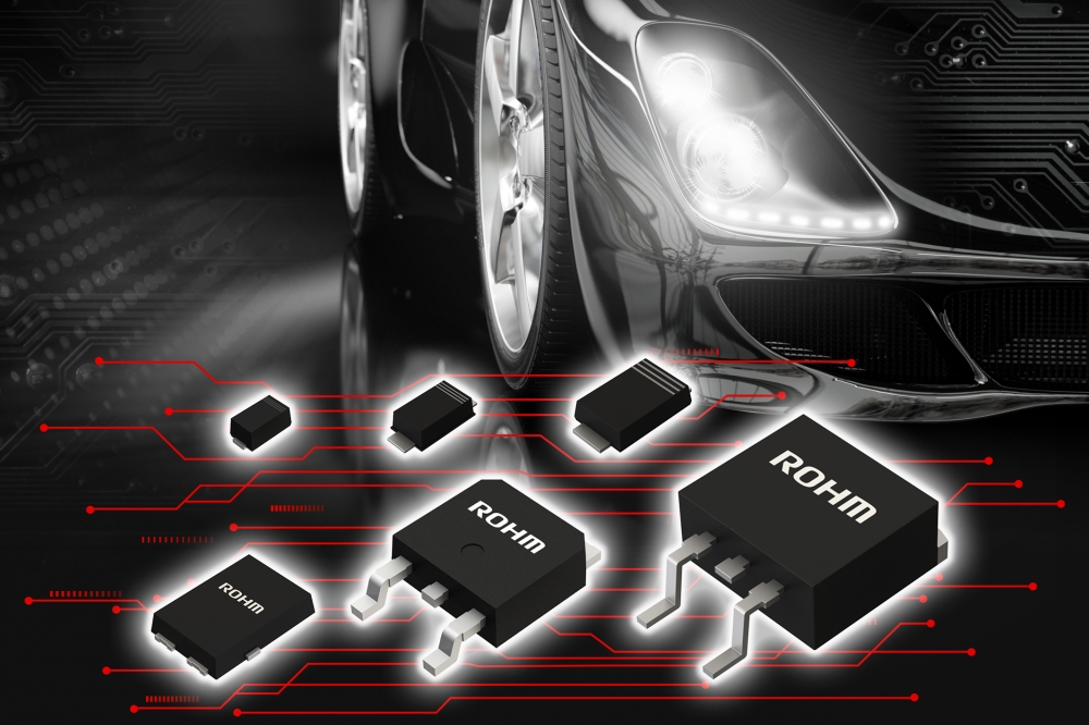
Ideal for automotive LED headlamps and other high-speed switching applications.
ROHM has developed 100V breakdown Schottky barrier diodes (SBDs) that deliver 'industry-leading' reverse recovery time (trr) for power supply and protection circuits in automotive, industrial, and consumer applications.
Although numerous types of diodes exist, highly efficient SBDs are increasingly being used inside a variety of applications. Particularly SBDs with a trench MOS structure that provide lower VF than planar types enable higher efficiency in rectification applications. One drawback of trench MOS structures, however, is that they typically feature worse trr than planar topologies – resulting in higher power loss when used for switching.
In response, ROHM developed a new series utilizing a proprietary trench MOS structure that simultaneously reduces both VF and IR (which are in a trade-off relationship) while also achieving class-leading trr.
Expanding on the four existing conventional SBD lineups optimized for a variety of requirements, the YQ series is ROHM’s first to adopt a trench MOS structure. The proprietary design achieves class-leading trr of 15ns that reduces trr loss by approx. 37% and overall switching loss by approx. 26% over general trench-type MOS products, contributing to lower application power consumption. The new structure also improves both VF and IR loss compared to conventional planar type SBDs. This results in lower power loss when used in forward bias applications such as rectification, while also providing less risk of thermal runaway which is a major concern with SBDs. As such, they are ideal for sets requiring high-speed switching, such as drive circuits for automotive LED headlamps and DC-DC converters in xEVs that are prone to generate heat.
Going forward, ROHM will strive to further improve the quality of its semiconductor devices, from low to high voltages, while strengthening its expansive lineup to further reduce power consumption and achieve greater miniaturization.
SBD Trench MOS Structure
The trench MOS structure is created by forming a trench using polysilicon in the epitaxial wafer layer to mitigate electric field concentration. This reduces the resistance of the epitaxial wafer layer, achieving lower VF when applying voltage in the forward direction. At the same time, during reverse bias the electric field concentration is minimized, significantly decreasing IR. As a result, the YQ series improves VF and IR by approx. 7% and 82%, respectively, compared to conventional products.
And unlike with typical trench MOS structures where trr is worse than planar types due to larger parasitic capacitance (resistance component in the device), the YQ series achieves an industry-leading trr of 15ns by adopting a unique structural design. This allows switching losses to be reduced by approx. 26%, contributing to lower application power consumption.
Application Examples
• Automotive LED headlamps
• xEV DC-DC converters
• Power supplies for industrial equipment
• Lighting


