Arizona Commerce Authority allocates funding to NAU

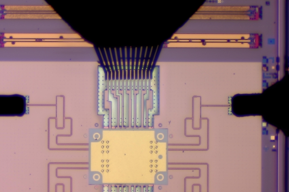
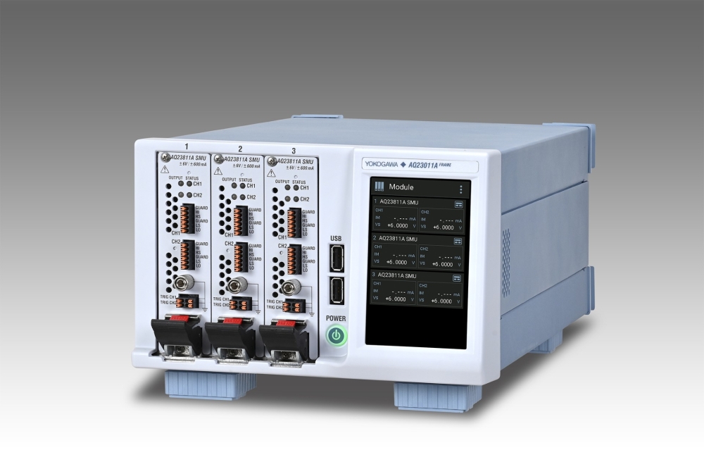
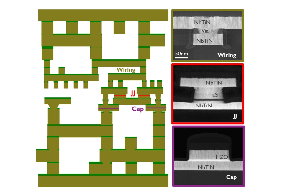
With $13 million in funds from the Arizona Commerce Authority (ACA), NAU is set to expand training programs and research related to metrology, a foundational component of semiconductor manufacturing and innovation.
Most of the electronic devices people use every day—from computers and smartphones to cars and major household appliances—require semiconductors to function. It’s no wonder, then, that state and educational leaders are working together to expand the American semiconductor industry by preparing future workers.
NAU will leverage the ACA investment to enhance Arizona’s semiconductor ecosystem, including establishing:
• A microelectronics metrology certificate program that will provide students with knowledge and skills in measurement and quality assurance;
• A semiconductor training center at the university’s North Valley Campus in Phoenix serving microelectronic and semiconductor industries that require a skilled workforce; and
• A campuswide metrology research and teaching laboratory bringing subject matter expertise from multiple disciplines, including electrical engineering, computer engineering, mechanical engineering, MIRA, physics and chemistry.
CEIAS Dean Andy Wang and associate VPR Andy Koppisch at a signing ceremony with ACA and UA.
Metrology plays a central role in semiconductor manufacturing in areas of process control, yield improvement and quality assurance. The National Institute of Standards and Technology (NIST) reports that demand for metrology professionals in the semiconductor industry is rapidly outpacing supply, a gap that is expected to widen.
“Arizona’s thriving semiconductor industry, which is bolstered by our world-class universities and community colleges, is creating thousands of good-paying jobs and career advancement opportunities,” said Gov. Katie Hobbs. “This investment is about ensuring Arizonans have the skills and training to fill those jobs and will further support the growing semiconductor industry presence in Arizona.”
“Semiconductors are a critical part of the 21st-century economy, and it is important that Arizonans have access to high-quality, affordable programs to prepare them for jobs in engineering, quantum computing and the semiconductor industry,” said NAU President José Luis Cruz Rivera. “NAU is pleased to partner with the ACA to help produce the next generation of engineers, innovators and creators through these groundbreaking programs.”
“Arizona has not only become a central hub of semiconductor manufacturing, but for research and development as well,” said Sandra Watson, president and CEO of the Arizona Commerce Authority. “We’re proud to partner with NAU to advance metrology training and R&D within the state to fill a critical need within the semiconductor workforce and further advance our state’s chip leadership.”
The ACA’s investment in NAU is part of a $100 million commitment announced in 2022 to increase semiconductor and microelectronics development in the state.
In December, in partnership with Arizona State University and NXP Semiconductors, the ACA announced a $17.5 million investment for ASU to expand advanced packaging and gallium nitride manufacturing research. The investment will further support Arizona’s advanced packaging capabilities.
In November, the University of Arizona and the ACA announced an expansion of the University’s Micro/Nano Fabrication Center (MNFC) in Tucson. The MNFC is a cleanroom facility which supports manufacturing and research efforts involving semiconductors, computer chips, optical devices and quantum computing systems. The MNFC expansion, which is supported by a $35.5 million investment from the ACA, will also include additional training efforts to continue growing the state’s skilled workforce.
In July, ASU, Applied Materials, Inc. and the ACA announced plans to create a world-class shared research, development and prototyping facility, the Materials-to-Fab (MTF) Center in the university’s MacroTechnology Works building at ASU Research Park. The MTF Center, which is supported by a $30 million investment from the Arizona Commerce Authority, will be home to Applied Materials’ Center of Excellence in materials deposition technology.


