DuPont to showcase materials innovation for EUV lithography

DuPont has announced that research in materials for extreme ultraviolet (EUV) lithography and advancing sustainability will be the focus of its technical presentations at SPIE Advanced Lithography + Patterning in San Jose, Calif., starting Feb. 25.
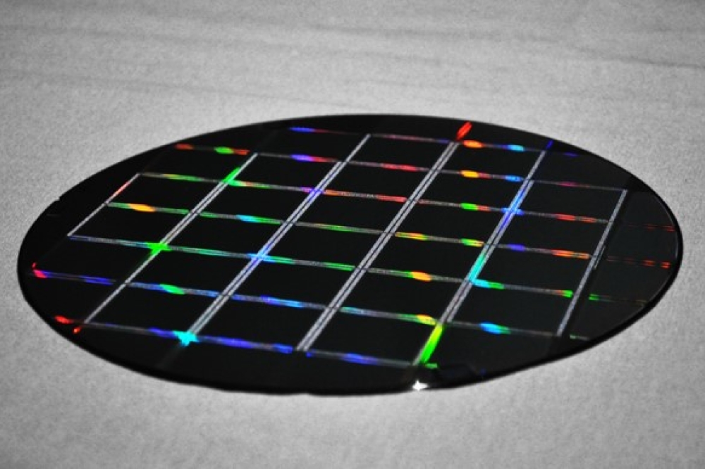
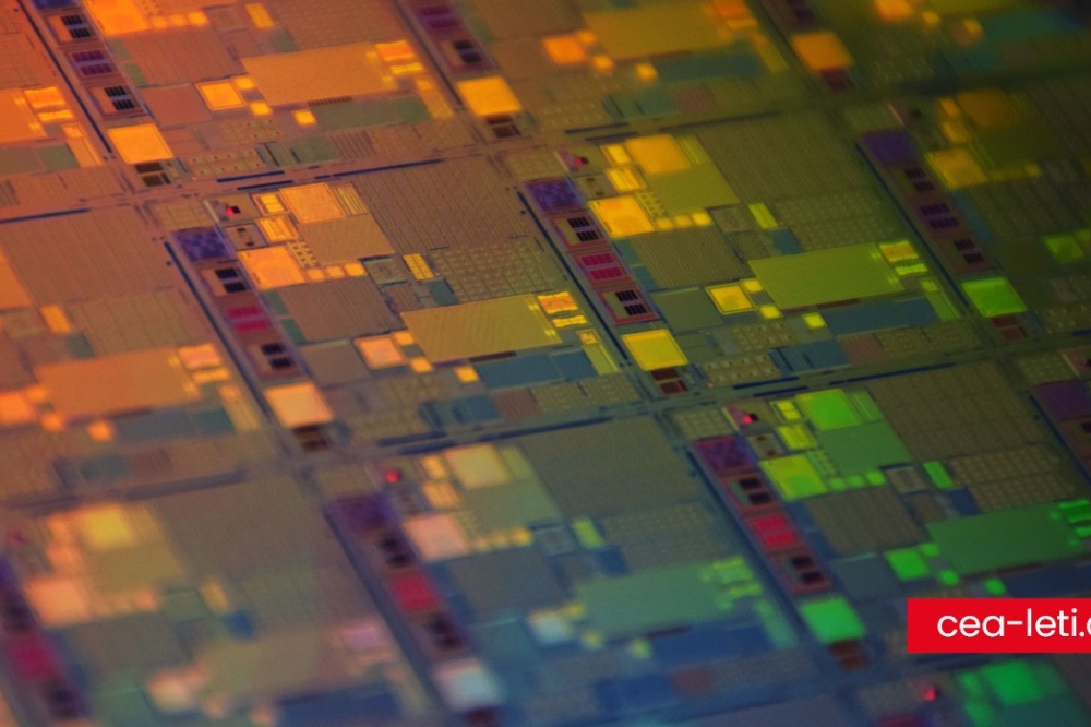
EUV lithography is a state-of-the-art imaging process for advanced semiconductor fabrication that uses light at a wavelength of just 13.5 nanometers to pattern nanoscale circuit designs. The use of EUV is enabling a continuation of semiconductor scaling by developing smaller, faster and more powerful integrated circuits to support advancements in high-performance computing applications like artificial intelligence and data centers.
“DuPont is extremely proud to be one of the leading innovators in materials for EUV lithography,” said Drew Chambers, Global Business Director, Lithography Technologies, DuPont Electronics & Industrial. “Building on a legacy of more than 50 years of materials innovation across lithography technologies, our team is now working with customers to enable today’s most advanced EUV lithography processes, including development of EUV underlayers and photoresists.”
As the adoption of EUV lithography progresses, there are many technical challenges to overcome. DuPont’s technical experts will share insights from research and development into materials for EUV, including solutions to improve resolution, line width roughness, and sensitivity. These include design strategies for chemically amplified photoresists, and production and filtration methods.
DuPont’s presentations on advancing sustainability showcase progress in reducing and eliminating the use of substances of concern in semiconductor materials formulation. Aligned with DuPont’s sustainability goals, and supporting customers with their own sustainability goals, DuPont is driving innovation in materials that are safe and more sustainable by design. Presentations will highlight innovation strategies for reducing substances of concern, including the development of non-fluorinated photoacid generators, the development of non-fluorinated surface leveling agents, and the development of photoresist formulations with these novel components.
“Sustainability is an important driver in DuPont’s innovation strategy, and our team has made incredible breakthroughs in developing novel solutions for lithography that deploy alternative, safe by design formulations,” said Ben Xie, Global R&D Director, Lithography Technologies, DuPont Electronics & Industrial. “We’re looking forward to sharing these efforts at the upcoming SPIE Advanced Lithography + Patterning conference to help accelerate sustainable design of materials across the semiconductor industry.”
DuPont’s presentations are part of the Advances in Patterning Materials and Processes Conference. Dr. Xisen Hou, Technical Manager, DuPont Electronics & Industrial, serves as a member of the Program Committee.

