Cadence and Intel Foundry collaborate

Collaboration enables heterogeneous integration with EMIB packaging technology.
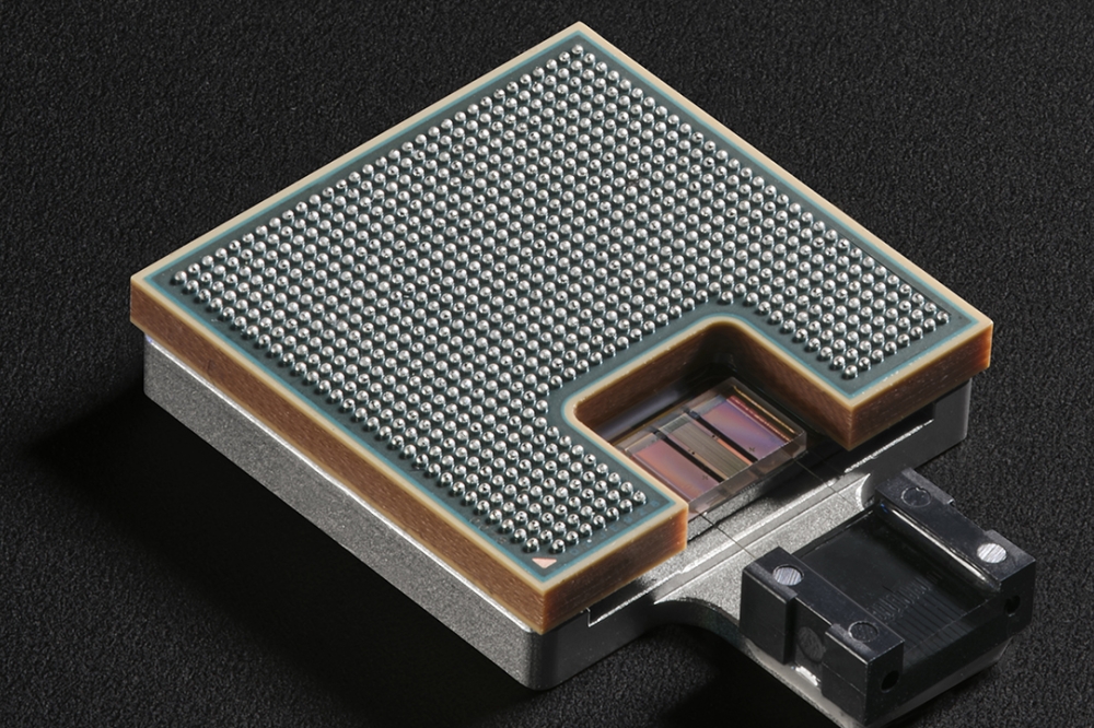
Cadence and Intel Foundry have collaborated to develop and certify an integrated advanced packaging flow utilizing Embedded Multi-die Interconnect Bridge (EMIB) technology to address the growing complexity in heterogeneously integrated multi-chip(let) architectures. The collaboration enables Intel customers to leverage advanced packaging to accelerate the high-performance computing (HPC), AI, and mobile computing design space. The advanced EMIB flow enables design teams to seamlessly transition from early-stage system-level planning, optimization and analysis to DRC-aware implementation and physical signoff without converting data between different formats. This revolutionary collaboration promises to significantly reduce design cycles for complex multi-chip(let) packages.
The joint effort has resulted in an advanced packaging flow, including Cadence’s Allegro® X APD (for placement, signal/power/ground routing, in-design electrical analysis, DFM/DFA and final manufacturing output), Integrity™ 3D-IC Platform and Integrity System Planner (for system-level design aggregation, planning and optimization), Sigrity™ and Clarity™ solvers (for 3D EM extraction, two-parameter generation, early-stage and signoff signal integrity, DC/AC power analysis, and packaging model extraction), Celsius™ solvers (for early-stage and signoff thermal signoff/stress), Virtuoso® Studio (for signal/power/ground routing of EMIB bridges), and Pegasus™ Verification System (for signoff DRC and SystemLVS).
“As more designers turn to multi-chiplet architectures and advanced packaging, there’s more emphasis on having the right design tools and methodologies,” said Michael Jackson, Corporate Vice President of Research and Development, Custom IC and PCB Group at Cadence. “The Cadence collaboration with Intel helps streamline this transition to heterogeneous integrated solutions by offering an EMIB-certified reference flow. This optimized flow empowers our joint customers to swiftly navigate the complexities of modern electronics design in the fast-paced tech market.”
“Incorporating thermal, signal integrity and power modeling early in engineering projects' planning and implementation stages is crucial for a seamless design process,” said Rahul Goyal, Vice President and General Manager, Product and Design Ecosystem, Intel Foundry. “By integrating these considerations upfront, engineers can conduct concurrent design and signoff activities, which help to avert potential downstream delays. Moreover, this proactive approach confirms design viability and ensures consistent compliance with required standards and guidelines."
This strategic collaboration decidedly enables the customers and reduces risks for customers engaging with Intel technology.


