+44 (0)24 7671 8970
More publications     •     Advertise with us     •     Contact us
 
Loading...
News Article

New Wooptix Poster at SPIE Advanced Lithography and Patterning

News

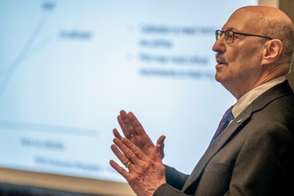
Jan O. Gaudestad will present the Poster “A new optical metrology technique for measuring the shape of a lithography photomask”.

SPIE Advanced Lithography and Patterning Conference, taking place between February 25th and February 28th in San Jose (California), will attract attention from the entire semiconductor lithography and metrology industry. Its lineup of speakers are world-class leaders such as Anne Kelleher from Intel Corp, Todd Younkin from Semiconductor Research Corporation, and Chan Hwang from Samsung.

As part of this significant event, Wooptix will present a poster titled "New optical metrology technique for measuring the shape of a lithography photomask." The presentation will take place on the 28th at 5:30 PM in the Convention Center, Hall 2.

Jan O. Gaudestad, VP Business Development Manager, states: "Wafer overlay errors due to non-flatness and thickness variations of a mask need to be minimized to achieve good on-product overlay (OPO). Due to the impact on overlay errors inherent in all reflective lithography systems, EUV reticles will need to adhere to flatness specifications below 10nm, values which are nearly impossible to meet using current tooling infrastructure with current state-of-the-art reticles reporting Peak-to-Valley (PV) flatness of around 60nm²."

Through Wooptix' poster, "We introduce a new technique, called Wave Front Phase Imaging (WFPI), that will generate a shape map with 810 thousand data points on an 86.4mm× 86.4mm area on an optical photomask with 96µm spatial resolution with a total data acquisition time of 14 seconds," Gaudestad emphasizes.

The team involved in the paper includes Guillermo Castro, Miguel Jiménez, Kiril Ivanov, Juan M. Trujillo, José Manuel Rodríguez Ramos, and Jan Olaf Gaudestad, who is also the presenter that day.

Jan O. Gaudestad is based in San Francisco, US, and is responsible of the VP of Business Development for Wooptix. Before Wooptix, he was Director of BD at a VR startup and prior he worked on strategic accounts for motion sensors at InvenSense/TDK. He spent 14 years at Neocera, a backend semiconductor equipment maker where he was part of the team raising $13 million in 2002 to commercialize his graduate research work.

Reality AI Explorer Tier offers free AI/ML development access
AEM introduces new generation of Automated Burn-In Systems
NPUs are emerging as the main rival to Nvidia’s AI dominance, says DAI Magister
Camtek receives a $20M order from a Tier-1 OSAT
Free samples of every STMicroelectronics NPI IC available from Anglia
NY CREATES and SEMI sign MoU
Major government investment to 'propel' Canada
QuickLogic announces $5.26 million contract award
ASNA and Athinia collaborate
Global sales forecast to reach record $109 billion in 2024
AMD to acquire Silo AI
Nanotronics unveils 'groundbreaking' Gen V AI Model
Aitomatic unveils SemiKong
Biden-Harris Administration reveals first CHIPS for America R&D facilities and selection processes
Collaboration to produce cutting-edge AI accelerator chips
Oxford Ionics breaks global quantum performance records
Adeia wins ECTC Award for paper on “Fine Pitch Die-to-Wafer Hybrid Bonding”
AEM introduces new generation of Automated Burn-In Systems
Sydney council forges vital semiconductor agreement
EV Group's EVG880 LayerRelease wins 2024 Best of West
Biden-Harris Administration to invest up to $1.6 billion
Cyient sets up subsidiary for semiconductor business
EMD Electronics network leaders honoured
Accenture acquires Cientra
Introducing Park FX200
Deep learning chipset market to surge to $72.8 billion by 2033
PI Innovation Award 2024: Nanobodies for Diagnostic and Therapeutic Applications
Graphcore joins Softbank Group
Kaman Measuring highlights high precision displacement sensors
Si2 reveals recipients of Annual Power of Partnerships Award
Advantest achieves ASPICE Level 2 Certification for V93000 SmarTest 8 Software
Semiconductors to become a trillion-dollar industry by 2030
×
Search the news archive

To close this popup you can press escape or click the close icon.
Logo
×
  • 1st January 1970
  • 1st January 1970
  • 1st January 1970
  • 1st January 1970
  • 1st January 1970
  • 1st January 1970
  • 1st January 1970
  • 1st January 1970
  • View all news 22645 more articles
Logo
×
Register - Step 1

You may choose to subscribe to the Silicon Semiconductor Magazine, the Silicon Semiconductor Newsletter, or both. You may also request additional information if required, before submitting your application.


Please subscribe me to:


You chose the industry type of "Other"

Please enter the industry that you work in: