Tata Group to build India’s first indigenous facility in Assam

INR 27,000 crore investment in a greenfield facility in Assam for assembly and testing of semiconductor chips for applications across automotive, mobile devices, artificial intelligence (AI), and other key segments to serve customers globally.
In a significant step towards creating an end-to-end semiconductor manufacturing ecosystem in India, Government of India has approved a proposal by Tata Electronics to build a state-of-the-art, greenfield semiconductor assembly and test facility in Jagiroad, Assam. The facility will be built with an investment outlay of INR 27,000 crore and is expected to generate over 27,000 direct and indirect jobs in the region.
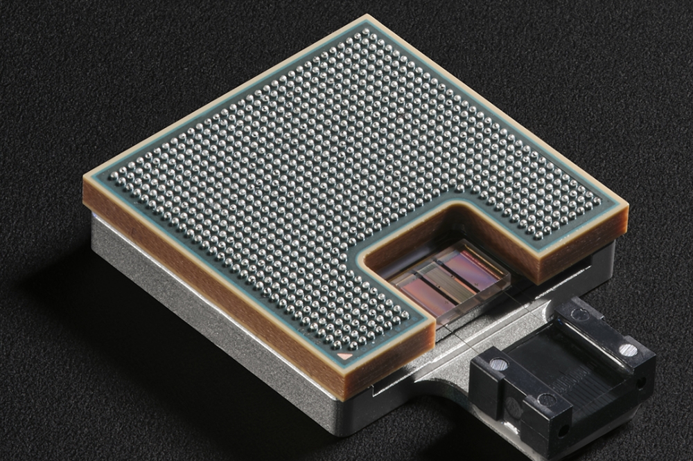
Tata Electronics Pvt Ltd (wholly owned subsidiary of Tata Sons Pvt Ltd) will build this facility focusing on three key platform technologies - Wire Bond, Flip Chip, and a differentiated offering called Integrated Systems Packaging (ISP), with plans of expanding the roadmap to advanced packaging technologies in the future. These technologies are extremely critical for key applications in India – like automotive (especially electric vehicles), communications, network infrastructure and others. Tata Electronics has already made significant investments in indigenous technology development for all these platforms and has put together a very credible team with over 1,000+ years of global domain experience to drive this project. The proposed facility will serve the growing global demands across key market segments like AI, industrial, and consumer electronics.
The construction of the facility is scheduled to start this year with the first phase of the facility becoming operational by mid-2025 and will provide an immense boost to industrialization in North-East India. The project is envisioned under the Government of India’s Semiconductor policy being driven by the India Semiconductor Mission and the Government of Assam’s Electronics policy.
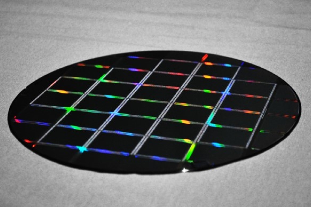
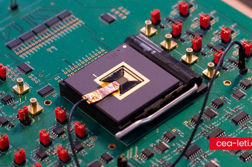
Semiconductor assembly and test is a critical part of the semiconductor value chain where wafers manufactured by semiconductor fabs are assembled or packaged and then tested before they are finally used in the desired product. Innovations in semiconductor assembly and test are driving increased performance, reduced form factor, and reduced costs of semiconductor chips.
Commenting on the announcement, N Chandrasekaran, Chairman, Tata Sons said, “We are in a unique time for the electronics manufacturing market globally and the world is seeking a more secure and resilient electronics supply chain. With our announcement of the semiconductor fab and this strategic project in semiconductor assembly and test, we will be enabling our global customers to base a key part of their semiconductor value chain in India. Alongside mitigating global supply chain risks, I am confident that this project will have a transformational impact towards technology led industrialization and job creation in the Northeast in particular.
Under the decisive leadership of Hon’ble Prime Minister Shri Narendra Modi, the Government of India has developed a comprehensive central and state semiconductor policy. This along with support from Ministry of Electronics and Information Technology, India Semiconductor Mission and the Government of Assam has made this announcement possible.”
Dr Randhir Thakur, CEO & MD, Tata Electronics said, “The strategy of serving across the semiconductor value chain is our differentiator and will enable Tata Electronics to deliver complete system offerings to customers. We have a critical window of opportunity where we see tremendous customer pull from global players for manufacturing in India and we plan to capitalize on this opportunity and leapfrog through technology innovation. This investment will go a long way in putting India on the map of global semiconductor manufacturing and in spurring a complete domestic ecosystem for high technology manufacturing while being an enabler for the indigenous product ecosystem.”
The proposed facility in Jagiroad is strategically located with access to abundant water and green power – a key sustainability consideration for the Tata group and its customers globally. Assam is also closer to the current semiconductor packaging & test hubs in countries like Taiwan, Malaysia, Vietnam, and Singapore. Assam has technical and engineering workforce available from the entire North-East India, providing a stable talent pool for this project as well as the ecosystem development that this project will seed. This new initiative from Tata Electronics will bring to India a portfolio of cutting-edge semiconductor technologies, advanced skill set and talent, and a network of semiconductor manufacturing suppliers and ecosystem partners, resulting in foundational development of indigenous semiconductor ecosystem in India. This Assembly & Test facility will be able to directly ship semiconductor chips to end-users and OEMs (Original Equipment Manufacturers) in India and the world.


