
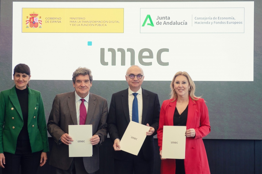
Spanish government, region of Andalusia and imec sign MoU
New R&D facility will complement imec’s 300mm cleanroom in Leuven with new processes and materials to boost innovation in upcoming domains such as health and augmented and virtual reality.
The Spanish government, together with the regional government of Andalusia and imec have signed a Memorandum of Understanding (MoU) outlining their intent to establish a specialized chip technology pilot line in Malaga (Andalusia). The new innovation facility intends to complement imec’s existing 300mm advanced CMOS process line in Leuven, Belgium, with new 300mm processes developments and the introduction of new materials that are difficult to combine today with standard CMOS processes. The new facility aims to answer the industry’s need for R&D, prototyping and pave the road to the manufacturing of promising, new technologies.
The facility aims to leverage the unique advantages of leading-edge 300mm semiconductor process technology to drive new applications in health care, life sciences, photonics, augmented and virtual reality, precision sensing, ... Complementing the existing expertise and infrastructure in Leuven with non-standard processes that are currently incompatible with semiconductor manufacturing processes, the two sites are meant to be closely linked.
The negotiations will now start with an eye to finding a strong public - private cooperation model, between imec, the Spanish government and the government of Andalusia. The governments already agree to support the construction of the new facility including the advanced equipment. They have also formulated the intention to financially support the pilot line’s operations in a sustainable, long-term manner, to the benefit of its growing semiconductor ecosystem. Imec intends to manage the operations, provide the required knowledge and technology, and guarantee access to its global academic and industrial partner network.
This MoU emphasizes the partners’ ambition to collaborate on a pan-European scale to contribute to the Spanish semiconductor ecosystem.
It builds on local strengths, yet leverages cross-border expertise and capabilities to address global societal challenges, while supporting regional economic ambitions. By establishing this new facility, which is closely connected to imec's Leuven-based 300mm pilot line, the goal is to fully harness the innovation potential in Spain and Andalusia.
Further details of the operations of the facility, such as hiring prospects, cannot be confirmed yet as they will be concluded in ensuing discussion.


