Loading...
News Article

scia System receives NIST order
News

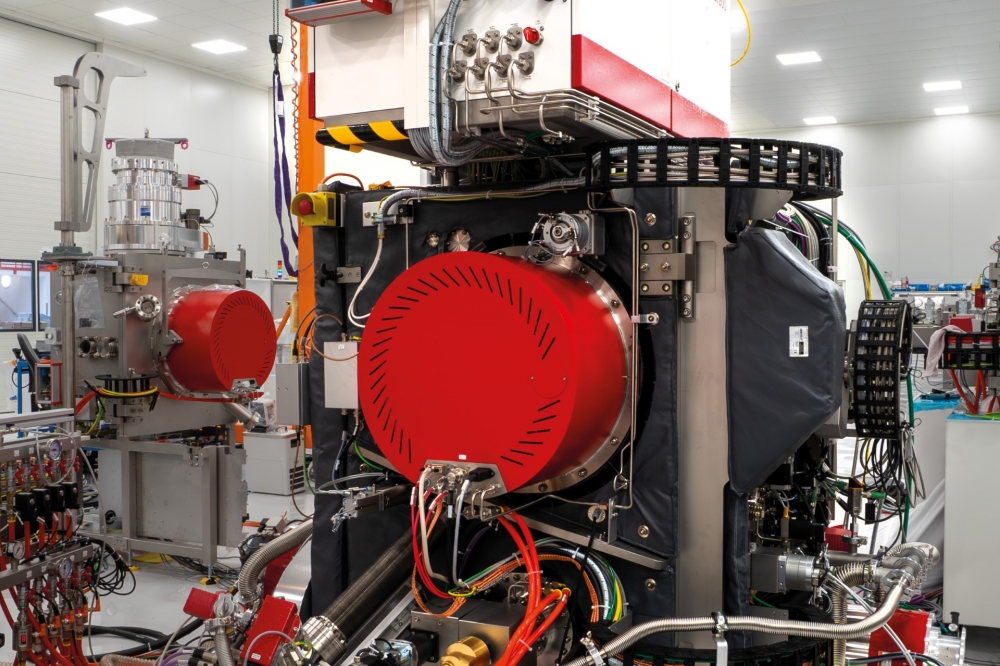
The scia Coat 200 system provides excellent uniformity for coating and etching processes using ion beam sputter deposition (IBSD) and ion beam etching (IBE).

The National Institute of Standards and Technology (NIST), one of the longest established physical science laboratories in the U.S., has purchased a scia Coat 200 system from scia Systems.

The customer will install the new scia Coat 200 in its Boulder Microfabrication Facility (BMF), a class 100 microelectronics processing facility. The state-of-the-art research laboratory supports the most sensitive research done at NIST to fabricate its next-generation microelectronic and microelectromechanical devices. The BMF will use the scia Coat 200 to deposit metals and dielectric materials as well as for the structuring of sensors and other devices.

High-Quality Multilayer Deposition with scia Coat 200

The scia Coat 200 uses ion beam sputtering (IBS) to achieve smooth, defect-free thin-film deposition. The IBS technology provides excellent uniformity for any coating by substrate rotation and tilt on up to 200 mm substrates. The system is equipped with a second ion beam source, used as an assist source, making the system capable of homogenous full surface ion beam etching. In-situ process control analysis ensures excellent process stability. The system enables the handling of wafers as well as arbitrarily shaped substrates.

A milestone for scia Systems

Although more than 500 advanced ion beam technologies of scia Systems have already been sold worldwide to industrial manufacturing and research institutes, this order marks a significant milestone for scia Systems and its local sales partner AARD Technology, LLC, because it is the first ion beam system sold to NIST. “We are pleased to have the opportunity to work with the BMF on their first installation and to support them to accelerate their path to production for their next-generation microelectronic and MEMS devices,” stated Dr. Michael Zeuner, CEO of scia Systems.

Silicon photonics: accelerating growth in the race for high-speed optical interconnects
CCD-in-CMOS technology enables ultra-fast burst mode imaging
2025 6G A look forward
Critical Manufacturing climbs Deloitte’s Technology Fast 50
Semiconductors: The most important thing you probably know the least about
Imec and partners unveil SWIR sensor with lead-free quantum dot photodiodes
Lattice introduces small and mid-range FPGA offerings
SEMI and SMT inspection solutions at NEPCON Japan 2025
Nordic Semiconductor and Kigen demonstrate Remote SIM Provisioning for Massive IoT
Spirent collaborates with Siemens
Quobly forges strategic collaboration with STMicroelectronics
New standards in pressure measurement systems for the semiconductor industry
IBM delivers optics breakthrough
Semiconductor equipment sales to reach $139 Billion in 2026
Marvell introduces 1.6 Tbps LPO Chipset
ACM research strengthens Atomic Layer Deposition portfolio
CEA-Leti demonstrates embedded FeRAM platform compatible with 22nm FD-SOI node
Lattice introduces small and mid-range FPGA offerings
Solace unlocks full potential of event-driven integration
Advantest to showcase latest test solutions at SEMICON Japan 2024
CEA-Leti device integrates light sensing and modulation
Nordic launches Thingy:91 X prototyping platform for cellular IoT and Wi-Fi locationing
Imec achieves seamless InP Chiplet integration on 300mm RF Silicon Interposer
High-precision SMU
Powering India’s energy future
China’s Nvidia probe puts global investors ‘on notice’
POET Technologies appoints new director
Imec demonstrates core building blocks of a scalable, CMOS-fab compatible superconducting digital technology
Imec proposes double-row CFET for the A7 technology node
ULVAC launches new deposition system
Beebolt and SEMI Announce Strategic Partnership to Drive Supplier Resilience and Agility
esmo group introduces Automated Final Test Manipulator
×
Search the news archive

To close this popup you can press escape or click the close icon.
Logo
x
Logo
×
Register - Step 1

You may choose to subscribe to the Silicon Semiconductor Magazine, the Silicon Semiconductor Newsletter, or both. You may also request additional information if required, before submitting your application.


Please subscribe me to:


You chose the industry type of "Other"

Please enter the industry that you work in: