Advanced packaging advances next wave of innovation in global chips manufacturing
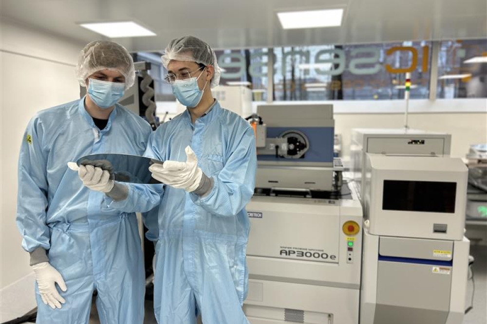
Arizona State University (ASU) and Deca Technologies (Deca)are collaborating to create North America’s first fan-out wafer-level packaging (FOWLP) research and development centre.
The new Center for Advanced Wafer-Level Packaging Applications and Development is set to catalyze innovation in the United States, expanding domestic semiconductor manufacturing capabilities and driving advancements in cutting-edge fields such as artificial intelligence, machine learning, automotive electronics and high-performance computing.
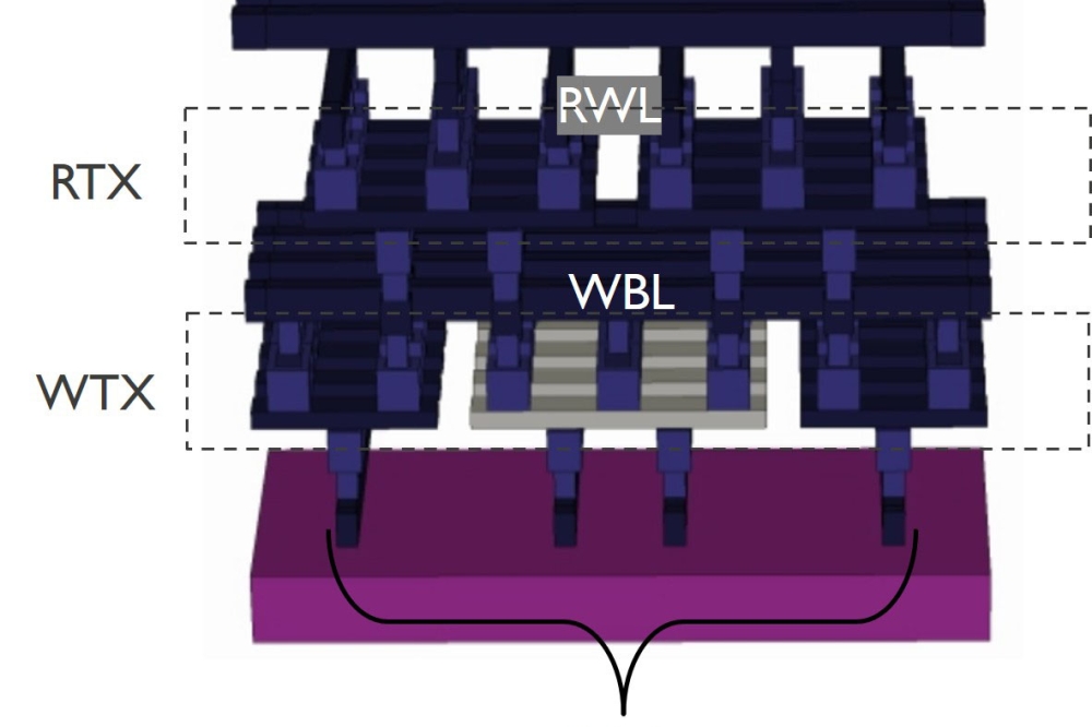
The center will combine state-of-the-art advanced-packaging technology, equipment, processes, materials, expertise and training, fostering the development of new capabilities from proof of concept to pilot scale. ASU is the first university implementation of Deca’s M-SeriesÔ fan-out and Adaptive Patterning® technologies under the Microelectronics Commons, a network of regional technology hubs coordinated to deliver on projects requested by the Department of Defense as part of the CHIPS and Science Act, the federal legislation which aims to expand America’s global leadership in microelectronics.
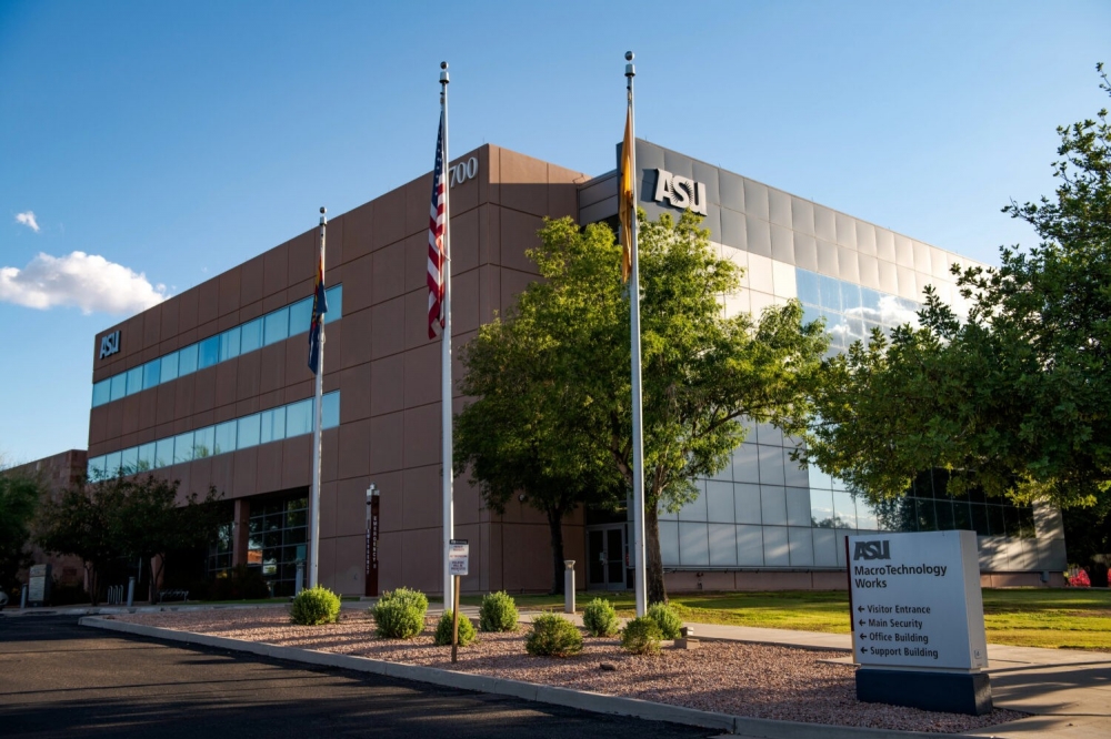
The new center will include integration with the university’s MacroTechnology Works center at ASU Research Park in Tempe and will provide enhanced capability that will advance projects within the ASU-led Southwest Advanced Prototyping (SWAP) Hub, part of the Microelectronics Commons.
“This is at the heart of the next generation of innovation in microelectronics and everything it enables,” said Zak Holman, vice dean for research and innovation for ASU’s Ira A. Fulton Schools of Engineering. “Deca has developed a unique technology, and ASU brings extraordinary capacity that will provide the resources to leverage Deca’s technology in ways that will be a differentiator for the work we are doing together through the SWAP Hub.”
The initiative also offers a workforce-development opportunity with ASU faculty and students engaging in the work being done, providing training for the growing number of technicians who are needed domestically, including in metro Phoenix, which is home to Intel, TSMC, Amkor and other companies.
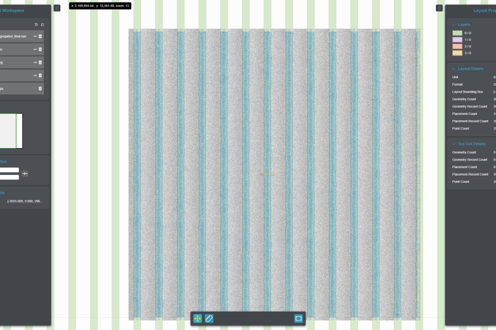
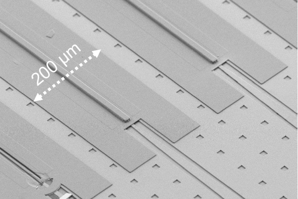
In collaboration with Deca, ASU is committed to establishing onshore access to these advanced-packaging capabilities. This entails acquiring, installing and implementing a comprehensive set of process and metrology equipment at the facility, capable of accommodating both 200mm and 300mm device wafer formats, as well as 300mm M-Series molded fan-out wafers, providing unparalleled flexibility for a diverse range of customers and applications.
“With the industry’s leading fan-out technology1 as a foundation, we’re excited about the possibilities this new center brings to Arizona as well as the broader U.S. semiconductor industry,” commented Tim Olson, Deca’s founder and CEO. “Through ASU and Deca’s collaboration, unprecedented access for industry, academia, government and others opens the door to accelerate innovation and bolster U.S. technology leadership.”
Deca’s first-generation M-Series FOWLP is widely adopted in leading smartphones around the globe. The Gen 2 M-Series including Adaptive Patterning technology brings unprecedented scaling to higher densities for heterogeneous integration and chiplet applications.