
Gel-Probe product line receives successful qualification
Gel-Pak has announced the successful qualification of its Gel-Probe product line by several of the semiconductor industry’s top tier probe card manufactures.
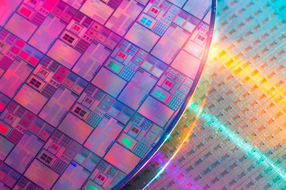
Gel-Pak has worked collaboratively with the industry’s leading probe card manufactures to optimize its suite of Gel-Probe products and successfully qualify them as appropriate for both the in-line and off-line cleaning of probe cards. The materials have been found to effectively clean probe tips, control contact resistance (Cres), and in many cases outperform other polymer-based probe card cleaning sheets and wafers.
Gel-Pak’s Gel-Probe products are the next evolution in probe card cleaning materials, available in both abrasive and non-abrasive sheets and wafers. GelProbe ReFine is an abrasive elastomer designed to eliminate embedded and bonded debris from probe tips, ensuring effective probe card cleaning and improved contact resistance (Cres). The non-abrasive Gel-Probe ReMove elastomer sheets and wafers effectively capture and remove loose debris that accumulates on the probe tip and electrical contact area during probing. Both products are suitable for all types of micro-cantilevered probe needles and MEMs springs, as well as advanced vertical and array technologies. Gel-Pak’s R&D team is continuing to collaborate with industry leaders on its next generation of probe cleaning technologies designed for greater efficiency and to ultimately reduce the overall cost of test.
"I'm excited about our ongoing partnership with leaders in semiconductor test to develop cutting-edge probe cleaning materials that address emerging needs, enhance efficiency, and optimize wafer yield. Together, we leverage innovation, expertise, and foresight to shape the trajectory of semiconductor testing, driving progress and excellence in the industry,” says Joe Montano, Delphon Industries President and CEO.
“Semiconductor manufacturers rely on a rigorous testing process to validate ‘good die’. Data integrity requires clean probes and reliable contact, making Gel-Pak's Gel-Probe a crucial part of efficient memory and non-memory device testing”, said Dr. Jerry Broz, VP of Strategic Marketing. “This probe cleaning solution streamlines failure identification, maximizing first-pass yield and throughput, ultimately reducing the overall cost of test. By working with leading technical partners, Gel-Pak is continuously innovating solutions for reliable and cost-effective wafer and device testing.”


