
Pragmatic welcomes HRH The Princess Royal
Site of the UK’s first 300mm semiconductor fabrication line (fab) delivering capacity to produce billions of flexible integrated circuits (FlexICs) per year.
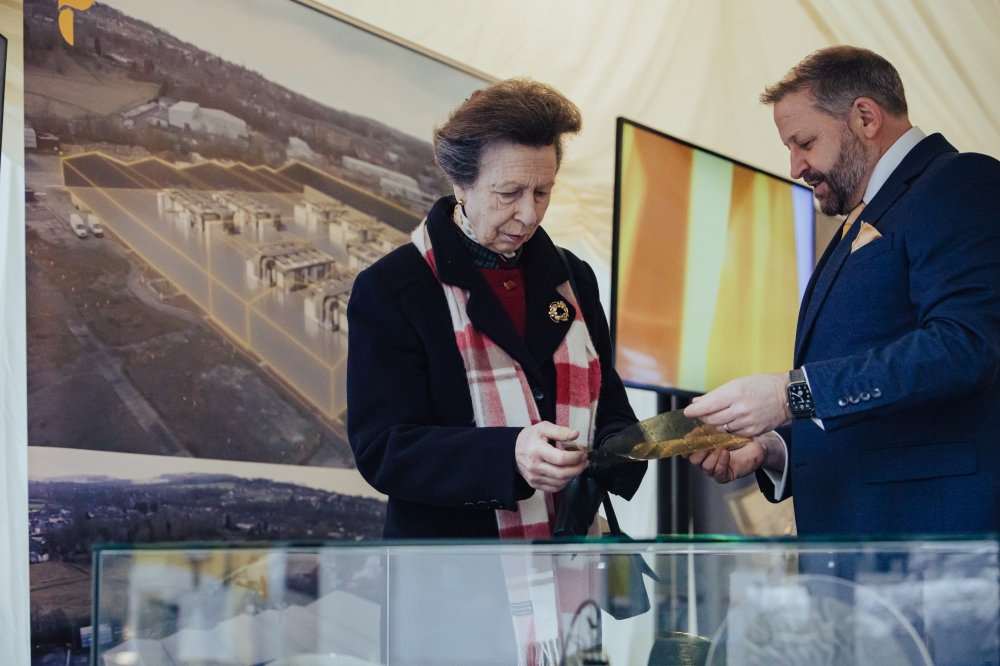
Pragmatic Semiconductor was recently honoured to welcome HRH The Princess Royal to officially open the UK’s first 300mm semiconductor wafer fabrication line (fab) at Pragmatic Park in Durham. The advanced manufacturing facility produces chips based on Pragmatic’s innovative and unique flexible integrated circuit technology. HRH The Princess Royal was hosted by David Moore, CEO, Pragmatic Semiconductor, with a tour of the clean room and facilities, followed by an unveiling of a site plaque to mark the occasion. Attendees included key customers, ecosystem partners, investors and government officials.
Pragmatic’s FlexICs are low-cost, more sustainable alternatives to silicon chips, ultra-thin, with a flexible form factor they enable connect, sense and compute capabilities, fuelling the Internet of Things (IoT) across multiple sectors including consumer, industrial, healthcare and beyond. The company’s mission is to provide item level intelligence to trillions of smart objects over the next decade across a wide range of applications with significant opportunities in smart packaging of fast-moving consumer goods that will significantly improve levels of reuse and recycling, transforming waste management, and enabling a circular economy. Other use cases include wearables, sensors and flexible controllers.
Pragmatic Park has capacity to host up to nine fabrication lines, each capable of producing billions of chips per year. Pragmatic’s pioneering sustainable approach extends to its manufacturing, using fewer process steps and a more concentrated footprint, than standard silicon fabs. The company’s innovative, optimised manufacturing process supports extremely rapid production cycles of less than 48 hours, at very low cost. The manufacturing process also uses significantly less energy and less water than typical silicon manufacturing, and fewer harmful gases. Pragmatic’s modular ‘Fab-in-a-Box’ approach, supports co-location of end-to-end FlexIC manufacturing at customers sites, rationalising extended supply chains and providing additional levels of security and resilience. The manufacturing facility enables the company to meet the growing demand for its unique technology from customers worldwide. Over the next five years Pragmatic anticipates creating over 500 highly skilled jobs in the North-East of England and Cambridge.
David Moore, CEO, Pragmatic Semiconductor said: "Today’s official opening marks a key milestone in Pragmatic’s growth trajectory and for the UK on the global semiconductor stage. I am incredibly proud of what the team has achieved and the ambition of our mission to enable item level intelligence in over a trillion sustainable, smart items over the next decade. Such intelligence at scale has the power to accelerate the digital transformation across industries. Sustainability is at the very core of our technology and extends to how FlexICs enable our customers to further drive innovations and pathways through their products and services towards global net zero goals.”
Francisco Melo, President Solutions Group, Avery Dennison commented: “The key to any effective collaboration is a shared mindset. Pragmatic’s innovative approach is reflective of our own, as is its commitment to helping solve business challenges. The opening of an advanced manufacturing chip facility is fantastic news for all technology innovators. Congratulations to Pragmatic on such an important and impressive achievement. I look forward to our clients harnessing the potential of Pragmatic's flexible integrated circuits as part of our evolving inlay portfolio."
Simon Little, Banking & Investments Director, UKIB and Pragmatic Board member added: “The Bank invested in Pragmatic to support low carbon domestic manufacturing of semiconductors in the UK. The official opening of Pragmatic Park in Durham marks a pivotal next step in its journey, and we look forward to seeing the long-term impact of our investment, as Pragmatic scales up its operation and creates highly skilled jobs here in the North-East.”
Niranjan Sirdeshpande, Global Head of M&G’s Catalyst strategy and Pragmatic Board member said: “The UK has a very supportive ecosystem for providing early-stage funding, but it becomes challenging for businesses looking for later stage capital. By providing growth equity to enterprising tech disruptors such as Pragmatic, M&G’s £5 billion Catalyst strategy can help them to scale, provide expertise and partner with them all the way to success. Put to work in this way, patient capital can support economic growth and capture value for peoples' pensions and savings as we transition to a more sustainable economy. We are proud to support Pragmatic’s work in Durham with tech advancement in this critical part of the UK's national infrastructure.”


