Manufacturing innovation centre focuses on electrification
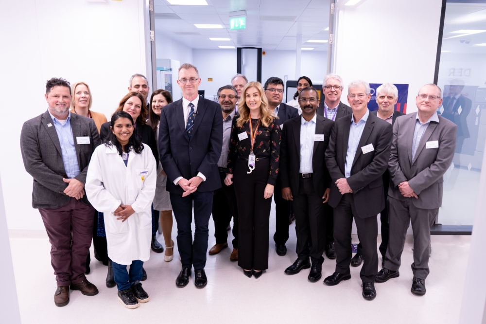
The Driving the Electric Revolution Industrialisation Centre (DER-IC) South West and Wales has opened its doors to industry, academia, and government.
DER-IC South West and Wales hosted the Secretary of State for Wales, David TC Davies, for the official opening of its advanced packaging facility at the Compound Semiconductor Applications (CSA) Catapult’s Innovation Centre in Newport.
DER-IC South West and Wales is part of the wider DER-IC network, which has four centres across the UK and offers open access equipment, facilities, and expertise to the Power Electronics, Machines and Drives (PEMD) manufacturing supply chain. PEMD are underpinning technologies that support electrification and will, in turn, enable Net Zero and boost the UK economy.
The official opening included a tour of the new facilities and keynote speeches from Jayakrishnan Chandrappan, Head of Advanced Packaging at CSA Catapult and Paul Jarvie, DER-IC South West and Wales Centre Lead. The speakers highlighted the capabilities of the new equipment and the specialist expertise that is available at CSA Catapult.
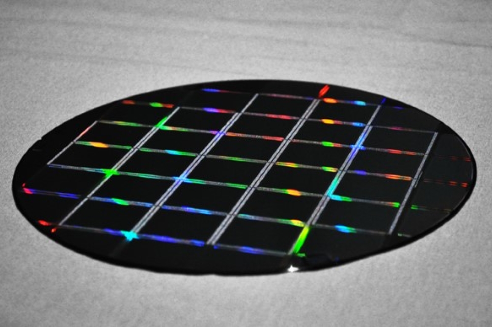
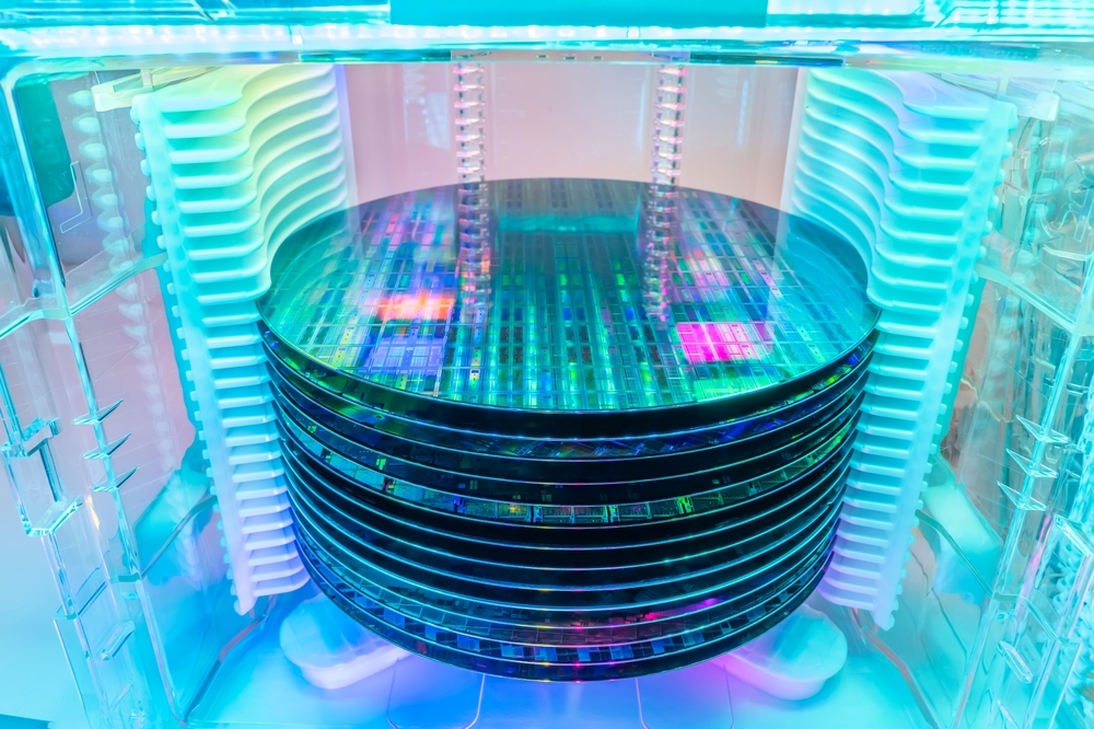
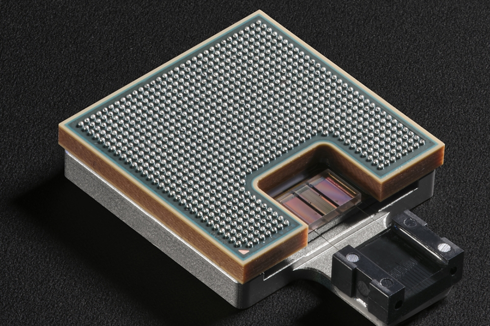
The new DER-IC South West and Wales facility can be used by manufacturers as a prototype facility for developing semiconductor and compound semiconductor packages using multi-material 3D printing, such as ceramic and metals.
Semiconductors, along with quantum, AI, engineering biology, and future telecoms, are recognised as transformative technologies. They are critical to the UK’s economic and national security.
These new facilities will support the UK government to deliver its National Semiconductor Strategy, a policy paper outlining how the UK will realise its ambitions to become a science and technology superpower. The strategy builds on the UK’s foundations and strengths in semiconductor technology.
Welsh Secretary David TC Davies said: “It was a fascinating visit to the DER-IC and see this brilliant resource for UK PEMD manufacturers. The UK Government is proud to support the compound semiconductor cluster in south Wales, which is vital to our ambition for the UK to lead the world in science and technology. The processes being developed here means that the supply chain within the UK is strengthened, helping to protect the industry and fostering job creation.”
The equipment showcased at the launch event included the centre’s advanced 3D printing equipment suite. The equipment is the UK's first in an open-access setting and stands as a pioneering facility. The equipment enables the integration of combination, mixed metal, and ceramic printing technologies for chip packages, heat sinks, and printed circuit board (PCB) designs.
The equipment includes:
A multi-material 3D printer that can quickly prototype novel packages using ceramic and mixed material for higher power and performance packaging
A 3D metal printer which can create fast prototypes for embedded packages and modules using copper or other conductive materials
An optimised laser system that can dice semiconductors and process ceramic or metal materials for novel package designs
The centre has already attracted significant interest from major industrial partners across the aerospace and transport sectors.
Dycotec Materials is looking to develop a 3D printing process to improve performance, reliability and significantly reduce the cost of packages and modules for automotive applications.
Meanwhile, CSA Catapult and Carbon Forest Products are involved in a project to create a 3D graphite heat sink - a key component used to move heat away from an electronic device - for use in automotive systems.
DER-IC South West and Wales Centre Lead Paul Jarvie commented: “The opportunities this centre presents to the PEMD manufacturing supply chain are significant. We’re inviting anyone in the PEMD supply chain who is interested in innovation and technology development, manufacturing scale-up and commercialisation, as well as skills and workforce development to engage with us.
“The new DER-IC facility, installed using the funding from the DER Challenge, allows industry to explore what materials it can use to create packaging that allows chips to reach their full potential within electric cars, trains, boats and other modes of transport. Our facilities can support manufacturers to de-risk innovation and attract investment in this area. We can help develop lighter, more energy-efficient components, which can handle more power, are less expensive, and can offer better overall thermal performance.”
Mike Biddle, Executive Director for Net Zero, Innovate UK said: “As key funders of both the CSA Catapult and DER-IC, Innovate UK is delighted to see the opening of the DER Lab in South Wales, a first in the UK. It shows the impact that different areas of the Innovate UK system coming together can have. It’s another example of how we are investing in cutting edge capability in Wales to meet the needs of businesses across the UK, and against the commitments we have made in our collaborative innovation plan for Wales. The Lab is a cutting-edge resource for industry to de-risk innovation and strengthen the supply-chain – this will be an invaluable facility for the semiconductor sector and the diverse PEMD community.”
Although this is the official centre launch, the doors to the facilities at DER-IC South West and Wales are already open and being utilised by PEMD manufacturers from across the UK.


