
Delivering RF Design Migration Flow to TSMC
New flow provides an efficient, integrated radio frequency circuit re-design solution based on Synopsys Custom Design Family, Keysight Electromagnetic Simulation, and Ansys Device Synthesis.
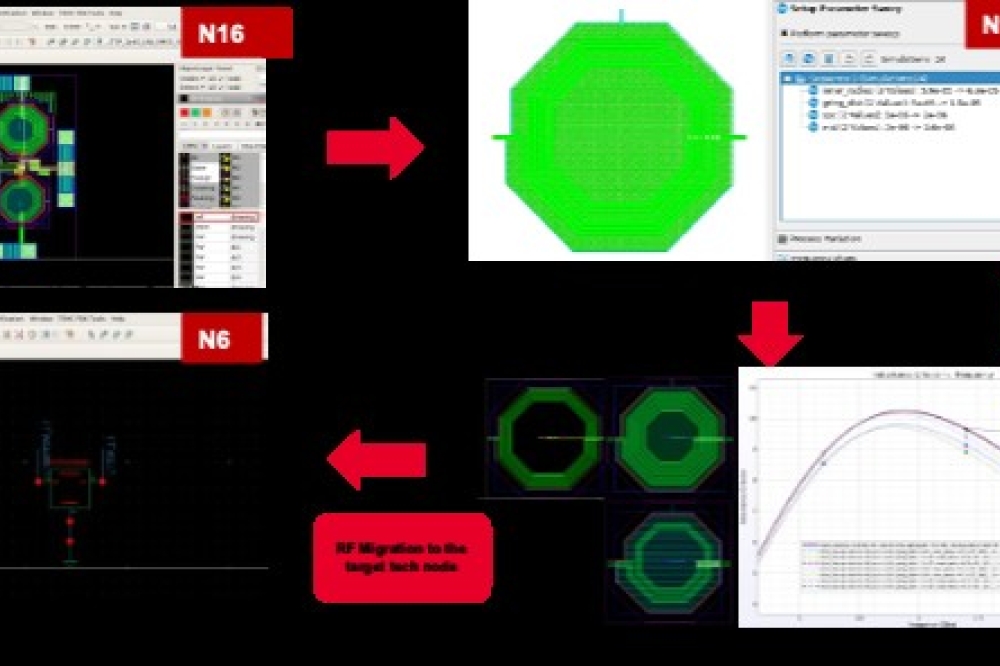
Keysight Technologies, Synopsys and Ansys introduce a new integrated radio frequency (RF) design migration flow from TSMC's N16 process to its N6RF+ technology to address the power, performance, and area (PPA) requirements of today's most demanding wireless integrated circuit applications. The new migration workflow integrates millimeter wave (mmWave) and RF solutions from Keysight, Synopsys, and Ansys into an efficient design flow that streamlines re-design of passive devices and design components to TSMC's more advanced RF process.
This RF design migration initiative extends TSMC's Analog Design Migration (ADM) methodology with additional capabilities for RF circuit designers. Beyond the productivity gains offered by ADM, the Keysight, Synopsys, and Ansys migration workflow demonstrates significant power reduction for a 2.4GHz low noise amplifier (LNA) design re-targeted to the N6RF+ process.
Key components of the design migration flow include:
• The Synopsys Custom Design Family, featuring Synopsys Custom Compiler™ layout environment with Synopsys ASO.ai™ for rapid analog and RF design migration and Synopsys PrimeSim™ circuit simulator
• Keysight RFPro for device parameterization, automated value fitting, and electromagnetic (EM) simulation
• Ansys RaptorH™ for on-silicon electromigration analysis and VeloceRF™ for passive component synthesis
RF circuit designers can adopt the migration flow to rapidly re-design their devices to the N6RF+ process specifications and accelerate time-to-market. Keysight RFPro enables parameterization of passive devices including inductors and automatically re-creates highly accurate simulation models with layout tuned to the new process. Designers view the re-created device layout in Synopsys Custom Compiler along with synthesized inductors from Ansys VeloceRF, and then perform interactive EM analysis in complex wireless chips.
Sanjay Bali, Vice President Strategy and Product Management EDA Group, Synopsys, said: "The need to rapidly migrate designs from node to node is essential to address the industry's relentless drive towards enhanced quality-of-results on TSMC's leading process technologies. The new flow, leveraging Synopsys' Custom Compiler, ASO.ai and PrimeSim solutions, offers an integrated RF and analog design migration solution that enables efficient migration of designs from TSMC N16 technology platform to N6RF+. Combining the strengths of trusted and industry-leading RF and mmWave solutions from Keysight, Synopsys and Ansys provides mutual customers with an interoperable design flow to unlock massive productivity gains."
Niels Faché, Vice President and General Manager, Keysight EDA, commented: "Meeting PPA requirements while adhering to new process design rules is one of the biggest challenges facing complex RF chip designs. RF circuit designers want to leverage and reuse their libraries of N16 device and component intellectual property to improve ROI. This new flow facilitates fast re-design in the latest TSMC N6RF+ technology for existing components originally built in N16. Keysight RFPro enables circuit designers to easily perform the device parameterization, new simulation model generation, and interactive EM analysis inside the Synopsys Custom Compiler layout environment. No time-consuming data handoffs or domain specialization are required, which increases overall engineering productivity for RF circuit designers."
John Lee, Vice President and General Manager of the Semiconductor, Electronics, and Optics Business Unit at Ansys, added: "Electromagnetic simulation and modeling play a central role in developing predictively accurate solutions for RF, high-speed analog, HPC data transmission, 3DIC interconnect, and co-packaged optics. We take pride in our partnership with Keysight, Synopsys and TSMC, because it enables Ansys to nimbly address some of the most challenging problems in this rapidly evolving and dynamic market. By fostering open platforms that integrate best-of-breed solutions, our joint customers will derive greater value and achieve enhanced product outcomes."
Dan Kochpatcharin, Head of the Design Infrastructure Management Division at TSMC, concluded: "We're delighted about our recent collaboration with Ansys, Keysight and Synopsys, which offers our mutual customers an efficient pathway to migrate their designs to our more advanced processes, ensuring that they meet the stringent PPA requirements. We're committed to continuing our collaboration with our Open Innovation Platform® (OIP) ecosystem partners to enable customers' next-generation designs with solutions benefiting from the significant power and performance boost of our leading-edge technologies."


