CEA-Leti to report on latest packaging research
CEA-Leti will present seven papers and one poster on its latest developments in microelectronics packaging, including three covering 3-layer integration, at the Electronic Components and Technology Conference (ECTC), May 28-31, in Denver.
A pioneer in heterogeneous 3D integration, the institute enables the combination of More Moore and More than Moore technologies. 3D integration and advanced packaging technologies are becoming mainstream for modular, high-bandwidth, low power consumption and efficient system architectures from consumer and automotive applications to high performance computing (HPC) and edge AI multi-layer smart imagers developed in the frame of IRT Nanoelec.
From high-density interconnection (fine pitch hybrid bonding DtoW and WtoW) to ultra-thin stacking layer interconnection with high density TSV and low temperature process, CEA-Leti is pushing the limits of 3D integration. It also is preparing the next generation of quantum computing with a complete set of packaging technologies.
ECTC Papers / Poster
• “Aging Behaviour and Environmental Impact of Under Bump Metallurgies for Wafer Level Balling”
Session 37, poster #33
Wednesday, May 29 from 10:00 AM - 12:00 PM
• “3-Layer Fine Pitch Cu-Cu Hybrid Bonding Demonstrator With High Density TSV for Advanced CMOS Image Sensor Applications”
Session 8, paper #2
Wednesday, May 29 from 2:00 PM – 5:05 PM
• “Fine Pitch Nb-Nb Direct Bonding for Quantum Applications”
Session 11, paper #3
Wednesday, May 29 from 2:00 PM – 5:05 PM
• “Backside Thinning Process Development for High-Density TSV in a 3-Layers Integration”
Session 9, paper #6
Wednesday, May 29 from 2:00 PM – 5:05 PM
• “Process Development and Characterization of Ru-Based UBM for In Bumps Interconnects Integration for Quantum Assemblies”
Session 9, paper #7
Wednesday, May 29 from 2:00 PM – 5:05 PM
• “Copper Microstructure Optimization for Fine Pitch Low Temperature Cu/SiO2 Hybrid Bonding”
Session 15, paper #6:
Thursday, May 30 from 9:30 AM – 12:35 PM
• “Low Resistance and High Isolation HD TSV for 3-Layers CMOS Image Sensors”
Session 19, paper #2
Thursday, May 30 from 2:00 PM – 5:05 PM
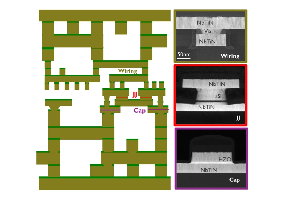
• “Integration of Planarized Nb-Based Vias to Form a Multi-Level Superconducting Back-End-of-Line”
Session 20, paper #1
Thursday, May 30 from 2:00 PM – 5:05 PM
Jean-Charles Souriau, a CEA project leader in the field of micro-interconnection and packaging, will co-chair a May 29 technical program, Sub-Micron Scaling in Wafer-to-Wafer Hybrid Bonding. The Session 8 program will run from 2:00 PM – 5:05 PM.
CEA-Leti experts will be onsite at booth 511 and available to discuss the findings in the presentations.

