
Lasers: a sustainable wafer heating solution
Lasers, in particular diode lasers, are an attractive and sustainable option for future chipmaking needs.
By Iurii Markushov, Kazunari Miyata and Harlon O. Neumann and Toby Strite, IPG Photonics Corporation
The journey to a sustainable fab requires closer examination of how silicon wafers are heated during chip making. Elevated wafer temperature is required for annealing, epitaxial and etch processes. A sustainable heating solution must minimize energy consumption and consumables, while providing excellent temperature uniformity and competitive thermal rise time. Heating by infrared laser has proven itself in other industries to be just such a silver bullet. Here we describe heating experiments on a 200 mm silicon wafer utilizing a commercially available 975 nm diode laser. An empirical thermal model enables extrapolation to 300 mm wafer heating scenarios. The experimental and theoretical findings coupled with the mature state of diode laser technology suggest that heating silicon wafers by laser is an attractive path forward.
Our experimental apparatus (Figure 1) projects an 11kW near infrared (975 nm) diode laser over a thermally isolated 200 mm polished silicon wafer in regular atmosphere. The projection optics uniformly illuminate a ~213 mm square fully covering the wafer surface with minimal energy overspill onto the heatsink beneath. Wafer temperature is measured using a Chino model IP-CZP0JL pyrometer positioned about one meter above the wafer. Our experiments operate the laser at constant output power until steady state temperature is reached. After laser power is shut off, the cooling curve is also recorded.

Figure 1. Experimental configuration showing the 11kW laser (right) and experimental chamber (left)
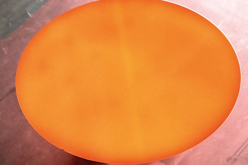
Maximum available 11 kW laser power heats the wafer quickly. Our experiment achieves 800°C in below 9 seconds. Steady state laser power of ~8.1 kW is sufficient to maintain that temperature. Figure 2 shows the heated wafer at 800°C. The color attests to the uniform nature of the laser heating across the wafer diameter.
Data were collected at six laser settings ranging from 0.86 kW to 8.1 kW constant power, enabling us to develop an empirical model covering a wide range of energy input, temperature and wafer diameters. The thermodynamic model incorporates absorptive heating from the laser, the wafer’s radiative and convective losses, and the heat capacity of silicon, each as a function of temperature.

Figure 2. Visible light image of 200 mm silicon wafer heated to 800°C by laser.
Figure 3 shows an example of fitting curves (blue – heating rise and steady-state and yellow - cooling) which accurately match experimental observations at 8.1 kW laser power. Similarly excellent fits were generated at the five other settings to create our temperature dependent empirical model.
Discussions with prospective customers suggest both the short rise times and low steady state power requirements demonstrated by the laser heater are highly attractive compared with infrared lamp alternatives. Fast rise times increase tool throughput. These are possible because up to 80% of the laser optical energy is absorbed by the silicon wafer. Low overall power requirements are a byproduct of the strong absorption, along with the high directivity of laser, meaning little energy is wasted heating the chamber atmosphere or enclosure. In contrast, infrared lamps operate hot, emit energy in all directions, and produce significant energy output at longer wavelengths where silicon is not highly absorbing.

Figure 3. Experimental (triangles) and modeled (blue and yellow) curves for 200 mm wafer heated by 8.1 kW of laser power
Figure 4 shows the calculated laser requirements to heat 300 mm silicon wafers to a variety of temperatures. The calculated values are modeled using a regular hexagonal illumination pattern such that 91.5% of the laser output hits the wafer surface. The first column provides the laser power required to heat the wafer to target temperature within a 10 second rise time constraint. Less power is required to hold a 300 mm wafer at the target temperature. The range of values required for steady state is given in the second column. The empirical model incorporates a temperature dependent absorption coefficient for silicon to match experimental data. At 400°C, we observe 62% of the laser energy is absorbed by the wafer, while at 800°C the absorbed percentage rises to 80%.
Commercially available diode lasers, such as the DLS-ECO series from IPG Photonics Corporation, are attractive options for the sustainable wafer fab. Silicon is absorptive at 975 nm, so up to 80% of the laser optical energy contributes to wafer heating. A diode laser converts 55+% of electrical power input to usable optical energy. Laser output is homogenized for uniform energy distribution, while its shape is tailored to match the wafer dimensions. Little energy is wasted heating the susceptor, chamber atmosphere or enclosure.

Figure 4. Table calculating laser power requirements to reach target
temperature in ten seconds, and maintain the target temperature. We
model a hexagonal laser illumination pattern (dark) which overspills
only 8.5% of laser energy off the 300m diameter wafer edge.
High component redundancy ensures diode lasers provide uninterrupted, service-free operation over seven years without any consumables. Fiber delivery cables 15 meters or longer enable laser light to be conveniently delivered to the tool, while all heat dissipation and electrical utilities remain outside the clean room. Because the laser operates at a single mid-infrared wavelength, pyrometry is effective in the absence of heater source interference.

While a laser is a higher up-front capital investment when compared to incumbent infrared lamp or inductive heaters, the premium is recoverable through reduced operational expense when we consider the unique combination of reliable, maintenance and consumable-free operation, low energy consumption and greenhouse gas footprint, along with the possibility to manage waste heat outside of the cleanroom. Lasers, in particular diode lasers, are an attractive and sustainable option for future chip making needs.


