
Inseto extends geographical reach
Inseto, technical distributor of equipment and materials, has been appointed Kulicke & Soffa’s exclusive distributor for high-quality hubbed dicing blades in Austria, Germany, the Netherlands and Portugal.
This appointment extends Inseto’s geographical remit as the company has been supplying K&S dicing blades – as well as wire and wedge bonders, dispensing equipment and die bonders - in the UK and Ireland since 2008.
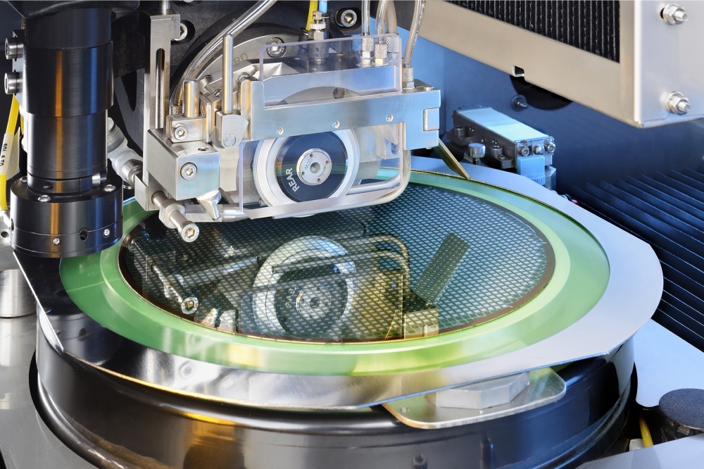
Hubbed dicing blades are used for cutting semiconductor wafers into individual die and are available with various grit sizes, diamond concentrations and binder hardnesses.
“We’re delighted to have been appointed to distribute K&S’s high quality hubbed dicing blades in Austria, Germany, the Netherlands and Portugal,” comments Matt Brown, Director of Inseto. “These are countries in which our technical specialists are already well known and supporting customers active in semiconductor manufacturing.”
Inseto has been supporting companies in the UK and Ireland with dicing blades for 16 years and is well versed in all technical aspects of wafer dicing. For example, silicon is a relatively soft material and single pass cuts are possible in most cases whereas as compound semiconductors, such as silicon carbide and gallium nitride, are harder and more brittle, often requiring multiple cuts to minimise the risk of sidewall cracking and chipping.
Brown adds: “Cut quality is governed by the size of the diamonds in the blade, the rate at which the binder material releases them - i.e. blade wear – the RPM at which the blade is spun and the rate at which it is moved through the wafer. Cooling and the use of surfactants also have an effect on cut quality, so there are lots of permutations to consider, and having gone to the expense of fabricating wafers it is important not to damage any die during the dicing process.”
As a supplier of dicing saws and a variety of processing equipment, Inseto can also advise customers early on in their projects on issues such as optimum ‘street’ widths between die, as there is understandably a trade-off between getting as many die as possible on a wafer and being able to cut between them without causing damage. Inseto is also a supplier of semiconductor wafers and has a dedicated online store.
“Our appointment by K&S to distribute hubbed blades in four more countries in Europe is great news in itself,” concludes Brown, “but it’s also broader recognition that Inseto has in-house expertise in all aspects of semiconductor manufacturing and that we’re able to help customers achieve a great economy of scale and return on investment.”


