Loading...
Vendor View

World’s first hybrid bonding allrounder for 200 mm and 300 mm substrates

News

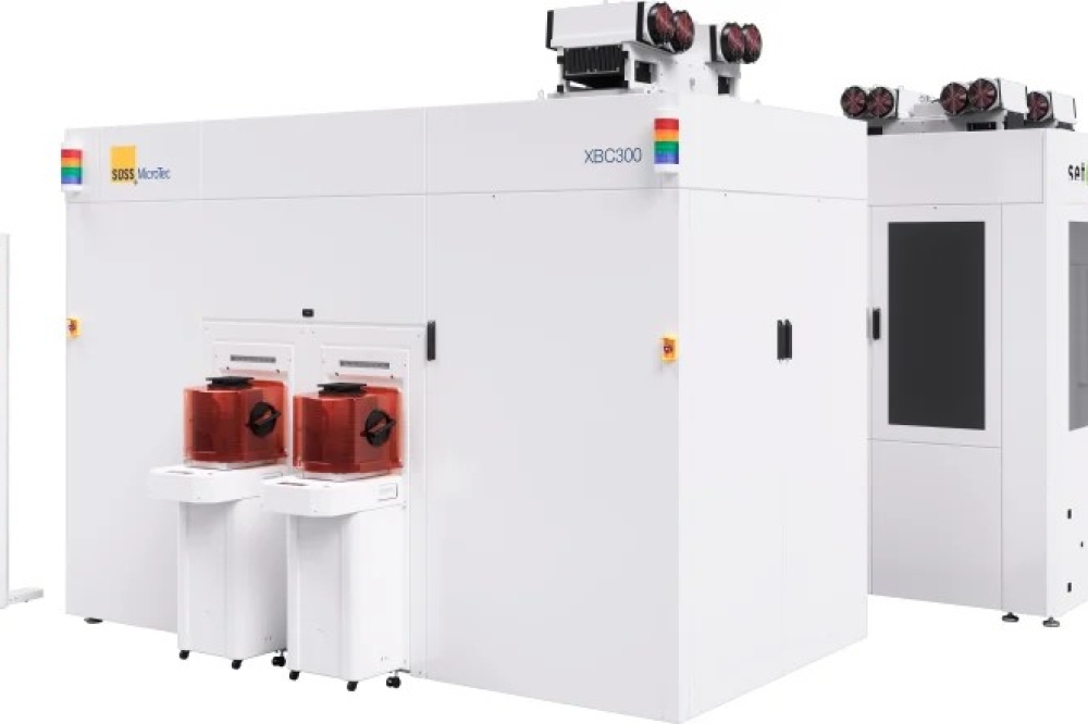
The new XBC300 Gen2 D2W/W2W cluster is the only platform in the world to integrate all existing hybrid bonding processes in a single tool: W2W, collective D2W and sequential D2W. The XBC300 Gen2 D2W/W2W is the result of a cooperation between SUSS MicroTec and SET Corporation SA, a supplier of high-precision flip-chip bonders. Compared to traditional stand-alone W2W and D2W clusters, the XBC300 Gen2 D2W/W2W offers a significantly reduced footprint. Investment costs are considerably lower because process modules that are redundant in separate stand-alone systems are only needed once. The XBC300 Gen2 D2W/W2W is a powerful and highly flexible universal platform that enhances hybrid bonding process development for advanced 3D stacking applications such as system-on-chip (SoC) and stacked IC (SIC).

Developed in close collaboration with our cooperation partner SET Corporation.

he XBC300 Gen2 D2W/W2W is specifically tailored to the needs of R&D lines or RTOs (research and technology organizations), who want to focus on one process first, but would like the option of developing further hybrid bonding processes in parallel or in the future. All process modules share the same core technology with dedicated stand-alone systems for D2W and W2W. This allows easy and reliable transfer from R&D to low and high-volume manufacturing.

In addition to the process modules required for W2W bonding with industry-leading alignment accuracy of < +/- 50nm, the XBC300Gen2 D2W/W2W features an integrated NEO HB die bonder from technology partner SET Corporation SA, offering +/-100nm alignment accuracy. A high-precision and throughput-optimized metrology station enables in-line verification of the alignment accuracy of both W2W and D2W bonds across all processes. Based on the XBC300 Gen2, an industry-renowned platform used by well-known major IDM customers in the field of temporary bonding, the XBC300Gen2 D2W/W2W allows for handling extremely thin microchips on tape frame carriers.

Silicon photonics: accelerating growth in the race for high-speed optical interconnects
CCD-in-CMOS technology enables ultra-fast burst mode imaging
2025 6G A look forward
Critical Manufacturing climbs Deloitte’s Technology Fast 50
Semiconductors: The most important thing you probably know the least about
Imec and partners unveil SWIR sensor with lead-free quantum dot photodiodes
Lattice introduces small and mid-range FPGA offerings
SEMI and SMT inspection solutions at NEPCON Japan 2025
Nordic Semiconductor and Kigen demonstrate Remote SIM Provisioning for Massive IoT
Spirent collaborates with Siemens
Quobly forges strategic collaboration with STMicroelectronics
New standards in pressure measurement systems for the semiconductor industry
IBM delivers optics breakthrough
Semiconductor equipment sales to reach $139 Billion in 2026
Marvell introduces 1.6 Tbps LPO Chipset
ACM research strengthens Atomic Layer Deposition portfolio
CEA-Leti demonstrates embedded FeRAM platform compatible with 22nm FD-SOI node
Lattice introduces small and mid-range FPGA offerings
Solace unlocks full potential of event-driven integration
Advantest to showcase latest test solutions at SEMICON Japan 2024
CEA-Leti device integrates light sensing and modulation
Nordic launches Thingy:91 X prototyping platform for cellular IoT and Wi-Fi locationing
Imec achieves seamless InP Chiplet integration on 300mm RF Silicon Interposer
High-precision SMU
Powering India’s energy future
China’s Nvidia probe puts global investors ‘on notice’
POET Technologies appoints new director
Imec demonstrates core building blocks of a scalable, CMOS-fab compatible superconducting digital technology
Imec proposes double-row CFET for the A7 technology node
ULVAC launches new deposition system
Beebolt and SEMI Announce Strategic Partnership to Drive Supplier Resilience and Agility
esmo group introduces Automated Final Test Manipulator
×
Search the news archive

To close this popup you can press escape or click the close icon.
Logo
x
Logo
×
Register - Step 1

You may choose to subscribe to the Silicon Semiconductor Magazine, the Silicon Semiconductor Newsletter, or both. You may also request additional information if required, before submitting your application.


Please subscribe me to:


You chose the industry type of "Other"

Please enter the industry that you work in: