
ERS electronic releases fully automatic Luminex machines with PhotoThermal debonding and wafer cleaning capability
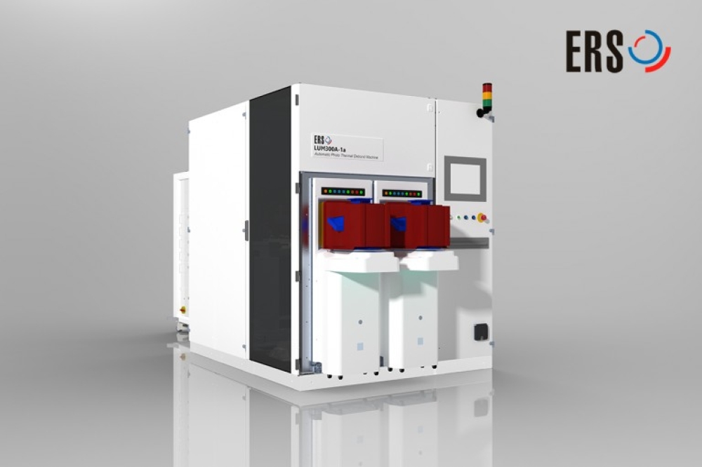
ERS electronic, in thermal management solutions for semiconductor manufacturing, has announced two new fully automatic machines from its Luminex product line. The machines, LUM300A1 and LUM300A2, are designed to handle 300 mm substrates and are both featuring ERS’s state-of-the-art PhotoThermal debonding technology that offers unparalleled flexibility, cost-effectiveness and throughput for temporary bonding and debonding processes.
“Temporary bonding and debonding is an indispensable technique for reliable substrate (wafer or panel) thinning and packaging,” asserts Taguhi Yeghoyan, PhD. Senior Technology & Market Analyst, Semiconductor Equipment at Yole Group. “Among all applications, recent advancements in packaging such as fan-out panel-level-packaging and heterogenous integration drive the temporary bonding and debonding equipment revenue that is expected to reach $571M in 2029, with a +16.6% CAGR 24-29, where more than 70% of revenue will be generated from laser-related machinery.”1
ERS’s new Luminex machines offer a unique solution for stress-free debonding, saving more than 30% in operation costs compared to traditional laser debonding. They are engineered with robust wafer handling capabilities, including thin wafers. The machines can boast with a throughput of >45 wafers per hour, providing a high-yielding solution that significantly enhances productivity.
A key advantage of the PhotoThermal debonding process is its compatibility with a wide range of bonding materials and suppliers, allowing the machines to cater to the high product variability of OSATs and to seamlessly integrate into various manufacturing workflows.
While LUM300A1 offers a high volume solution for the debonding process, LUM300A2 includes a wafer cleaning module to remove bonding adhesive remnants from the wafer.
“Our Luminex machines significantly enhance flexibility and efficiency in the debonding process, enabling our customers to accelerate the development of next-generation semiconductor chips for AI, automotive, and other cutting-edge applications,” says Debbie-Claire Sanchez, VP and Advanced Packaging Equipment BU Manager at ERS electronic.
The semi-automatic version, LUM600S1, for wafers and panels up to 600 x 600 mm was released to market in March and is available for test and evaluation in ERS’s competency centres in China and Germany


