
CEA-Leti reports three-layer integration breakthrough
CEA-Leti scientists reported a series of successes in three related projects at ECTC 2024 that are key steps to enabling a new generation of CMOS image sensors (CIS) that can exploit all the image data to perceive a scene, understand the situation and intervene in it – capabilities that require embedding AI in the sensor.
Demand for smart sensors is growing rapidly because of their high-performance imaging capabilities in smartphones, digital cameras, automobiles and medical devices. This demand for improved image quality and functionality enhanced by embedded AI has presented manufacturers with the challenge of improving sensor performance without increasing the device size.
“Stacking multiple dies to create 3D architectures, such as three-layer imagers, has led to a paradigm shift in sensor design,” said Renan Bouis, lead author of the paper, “Backside Thinning Process Development for High-Density TSV in a 3-Layer Integration”.
“The communication between the different tiers requires advanced interconnection technologies, a requirement that hybrid bonding meets because of its very fine pitch in the micrometer & even sub-micrometer range,” he said. “High-density through-silicon via (HD TSV) has a similar density that enables signal transmission through the middle tiers. Both technologies contribute to the reduction of wire length, a critical factor in enhancing the performance of 3D-stacked architectures.”
‘Unparalleled Precision and Compactness’
The three projects applied the institute’s previous work on stacking three 300 mm silicon wafers using those technology bricks. “The papers present the key technological bricks that are mandatory for manufacturing 3D, multilayer smart imagers capable of addressing new applications that require embedded AI,” said Eric Ollier, project manager at CEA-Leti and director of IRT Nanoelec’s Smart Imager program. The CEA-Leti institute is a major partner of IRT Nanoelec.
“Combining hybrid bonding with HD TSVs in CMOS image sensors could facilitate the integration of various components, such as image sensor arrays, signal processing circuits and memory elements, with unparalleled precision and compactness,” said Stéphane Nicolas, lead author of the paper, “3-Layer Fine Pitch Cu-Cu Hybrid Bonding Demonstrator With High Density TSV For Advanced CMOS Image Sensor Applications,” which was chosen as one of the conference’s highlighted papers.
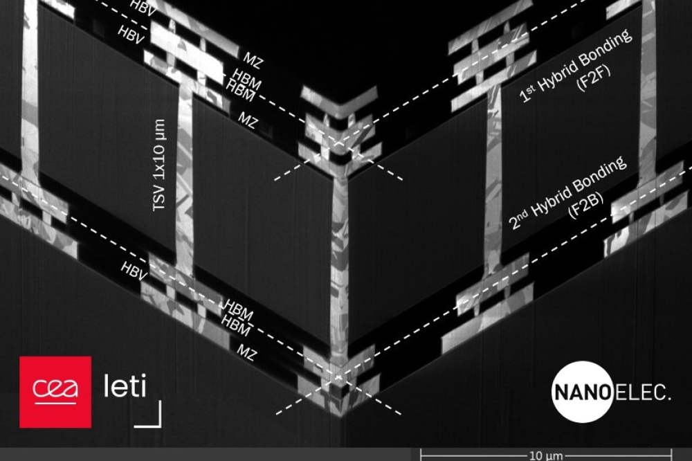
The project developed a three-layer test vehicle that featured two embedded Cu-Cu hybrid-bonding interfaces, face-to-face (F2F) and face-to-back (F2B), and with one wafer containing high-density TSVs.
Ollier said the test vehicle is a key milestone because it demonstrates both feasibility of each technological brick and also the feasibility of the integration process flow. “This project sets the stage to work on demonstrating a fully functional three-layer, smart CMOS image sensor, with edge AI capable of addressing high performance semantic segmentation and object-detection applications,” he said.
At ECTC 2023, CEA-Leti scientists reported a two-layer test vehicle combining a 10-micron high, 1-micron diameter HD TSV and highly controlled hybrid bonding technology, both assembled in F2B configuration. The recent work then shortened the HD TSV to six microns high, which led to development of a two-layer test vehicle exhibiting low dispersion electrical performances and enabling simpler manufacturing.
’40 Percent Decrease in Electrical Resistance’
“Our 1-by-6-micron copper HD TSV offers improved electrical resistance and isolation performance compared to our 1-by-10-micron HD TSV, thanks to an optimized thinning process that enabled us to reduce the substrate thickness with good uniformity,” said Stéphan Borel, lead author of the paper, “Low Resistance and High Isolation HD TSV for 3-Layer CMOS Image Sensors”.
“This reduced height led to a 40 percent decrease in electrical resistance, in proportion with the length reduction. Simultaneous lowering of the aspect ratio increased the step coverage of the isolation liner, leading to a better voltage withstand,” he added.
“With these results, CEA-Leti is now clearly identified as a global leader in this new field dedicated to preparing the next generation of smart imagers,” Ollier explained. “These new 3D multi-layer smart imagers with edge AI implemented in the sensor itself will really be a breakthrough in the imaging field, because edge AI will increase imager performance and enable many new applications.”


