
Doubling throughput of layer transfer technology
Dedicated HVM equipment platform boosts productivity and lowers cost-of-ownership of novel infrared laser release technology through silicon carrier wafers for 3D integration applications.
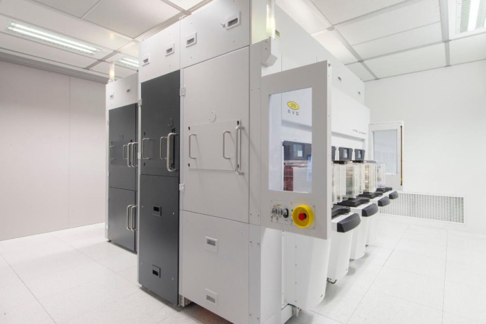
EV Group (EVG) has introduced the EVG®880 LayerRelease™ system, a dedicated high-volume manufacturing (HVM) equipment platform incorporating EVG’s innovative infrared (IR) LayerRelease™ technology. Providing a two-fold increase in throughput compared to the previous-generation platform, the EVG880 LayerRelease system enables nanometer-precision release of bonded, deposited or grown layers from silicon carrier substrates using an IR laser coupled with specially formulated inorganic release materials. As a result, the EVG880 LayerRelease system eliminates the need for glass carriers—enabling ultra-thin chiplet stacking for advanced packaging, as well as ultra-thin 3D layer stacking for front-end processing, including advanced logic, memory and power device formation, to support future 3D integration roadmaps.
Moving Beyond Glass Carriers for 3D Stacking
In 3D integration, glass substrates have become an established method for building up device layers through temporary bonding with organic adhesives, using an ultraviolet (UV) wavelength laser to dissolve the adhesives and release the device layers, which are subsequently permanently bonded onto the final product wafer. However, glass substrates are difficult to process with semiconductor fab equipment that have been designed primarily around silicon, and that require costly upgrades to enable glass substrate processing. In addition, organic adhesives are generally limited to processing temperatures below 300°C, limiting their use to back-end processing.
EVG’s LayerRelease technology utilizes an IR laser and inorganic release materials to enable laser debonding on silicon carriers with nanometer precision in production environments, thereby avoiding these temperature and glass carrier compatibility issues. The innovative process eliminates the need for glass substrates and organic adhesives, enabling front-end process compatibility for ultra-thin-layer transfer and downstream processes. The nanometer precision of the LayerRelease process allows for processing extremely thin device wafers without changing processes of record. Subsequent stacking of such thin device layers enables higher-bandwidth interconnects and new opportunities to design and segment dies for next-generation, high-performance devices.
The most demanding front-end processing is supported by the LayerRelease technology’s high-temperature compatibility (up to 1000°C) while the room-temperature IR cleaving step ensures device layer and carrier substrate integrity. The layer transfer process also eliminates the need for expensive solvents associated with carrier wafer grinding, polishing and etching.
The EVG®880 LayerRelease™ system is a dedicated HVM equipment platform incorporating EVG’s innovative IR LayerRelease™ technology, providing a two-fold increase in throughput compared to the previous-generation platform. Source: EV Group.
The new EVG880 platform upon which the LayerRelease technology has been integrated into is wholly designed and dedicated for the LayerRelease process. It is a fully automated, front-end-compatible, HVM platform with integrated laser exposure, wafer cleaving and wafer cleaning all in one tool. The EVG880 features a low-maintenance laser source and complete process control with laser metrology at point of use.
“3D integration is increasingly important in optimizing the Power, Performance, Area and Cost (PPAC) metric in semiconductor design and manufacturing, as well as enabling roadmap continuation,” stated Paul Lindner, executive technology director at EV Group. “With 3D integration, there is no way around wafer bonding or layer transfer. EVG’s LayerRelease technology is a truly unique and universal layer transfer technology that has been adopted by industry-leading research institutes and device manufacturers to support a wide range of applications, from advanced packaging to 3D integration to future front-end-of-line scaling. As early adopters of our LayerRelease technology are expected to move quickly from industrial research to manufacturing, EVG has increased its focus on improving the technology’s productivity and cost of ownership. We are excited to now be able to offer this innovative technology on our new EVG880 HVM equipment platform, enabling customers to rapidly deploy the LayerRelease process for their current and next-generation product designs.”


