Flip-chip die bonder promises speed improvement
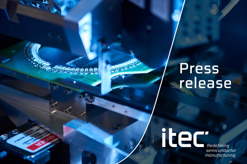
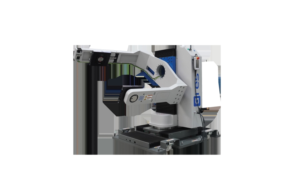
ITEC introduces the ADAT3 XF TwinRevolve flip-chip die bonder, said to run five times faster than existing machines, attaching up to 60,000 flip-chip dies per hour.
By enabling higher productivity with fewer machines, ITEC aims to help manufacturers reduce their factory footprint and running costs, thereby achieving a more competitive Total Cost of Ownership (TCO).
The ADAT3 XF TwinRevolve is designed with precision in mind with an accuracy better than 5 μm @ 1σ. This level of precision, combined with its ultra-high throughput, opens possibilities for a whole new generation of products where flip-chip assembly was previously too slow and too expensive. The use of flip-chip packages can also contribute to more reliable products with lower power consumption and better high-frequency and thermal management performance compared to traditional wire bonds.
Instead of the traditional forwards and backwards up/down linear motion, the new die bonder employs two rotating heads (‘TwinRevolve’) to pick, flip and place the die in a fast, smooth action. This unique mechanism reduces inertia and vibration, allowing for the same accuracy at much higher speeds. This development opens up new opportunities for chipmakers to transition their high-volume wire-bonded products to flip-chip technologies.
“We believe our new ADAT3 XF TwinRevolve flip-chip die bonder represents a significant step forward in the manufacturing of advanced flip chips and chiplets, aligning with the vision for the future of factory operations”, says Mark van Kasteel, Commercial Director at ITEC. “Its automated features, coupled with a design that requires significantly less space, contribute to a reduction in maintenance, operational hours, and energy consumption, ultimately leading to a smaller carbon footprint.”
FAST, AUTOMATED OPERATION
ITEC’s ADAT3 XF (eXtended Flexibility) range includes the market’s fastest and most advanced die bonders and die sorters. As with the whole ADAT3 XF (eXtended Flexibility) range, the new flip-chip die bonder stands out for its high speed and advanced features. Its modularity and field upgradability extend the machine’s operational lifetime thereby enhancing sustainability. An autoloader for strip magazines (in-outgoing) takes four magazines at a time with an option for E142 substrate mapping. There’s an automatic wafer change with barcode reader. The machine accepts 8- to 12-inch (200- to 300-mm) wafers. There’s full die traceability, auto recipe download (MES interface) and SECS/GEM interface.
A separate flux screen printer can be added as an inline-setup or the TwinRevolve can run as a standalone tool with strip magazine input/output, a flux screenprint inspection module is an option. Additionally, the die bonder is equipped with full servo-controlled bond-force/pick-force settings and auto-diagnostics to monitor machine health. Five high-resolution (up to 5 MPixel) cameras at key process points help keep operation under close control. They monitor glue, pre-pick, back/front side, post-bond and optional sidewall. Flux-related inspection includes drop size and shape, and coverage with respect to Cu pillar size.
WIDE RANGE OF PACKAGES
The die bonder takes several types of QFN, DFN, HVQFN, SOT, SO, TSSOP and LGA leadless and leaded packages, and can handle 100x300 mm strip size.

