
The future of flexible technology?
Organic electronics, a subfield of electronics that deals with conductive polymers and small organic molecules, is ushering in a new era of technological innovation.
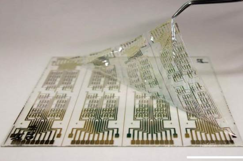
Unlike traditional electronics based on inorganic materials like silicon, organic electronics utilize carbon-based compounds, which offer unique advantages in terms of flexibility, weight, and cost.
Fundamentals of Organic Electronics
At its core, organic electronics relies on organic molecules that can conduct electricity. These molecules can be categorized into two main types: small molecules and polymers. Small molecules are usually crystalline and can be deposited in thin films through techniques like vacuum evaporation. Polymers, on the other hand, are long chains of repeating units that can be processed from solution, making them suitable for printing techniques.
The key to the functionality of organic electronic materials lies in their conjugated systems – structures with alternating single and double bonds. This arrangement allows electrons to move freely along the molecule, facilitating electrical conductivity. When these materials are doped with other substances, their conductivity can be significantly enhanced, making them viable for various electronic applications.
Advantages of Organic Electronics
1. Flexibility and Lightweight: One of the most notable advantages of organic electronics is the flexibility of the materials. This property opens up a range of possibilities for applications that require bendable or foldable components, such as wearable electronics, flexible displays, and rollable solar panels. Additionally, organic electronic materials are typically lighter than their inorganic counterparts, which is beneficial for portable and lightweight devices.
2. Low-Cost Production: Organic electronic materials can be processed at lower temperatures and with simpler techniques compared to traditional silicon-based materials. This reduces production costs and energy consumption. Techniques such as inkjet printing and roll-to-roll processing can be used to produce organic electronic devices on a large scale, making the technology accessible and economically viable.
3. Environmental Sustainability: Organic materials offer potential environmental benefits. They can be made from abundant raw materials and are often more environmentally friendly to manufacture and dispose of than traditional inorganic materials. Additionally, the lower energy requirements for processing further contribute to their sustainability.
Applications of Organic Electronics
The versatility of organic electronics has led to its application in a wide range of fields:
1. Organic Light Emitting Diodes (OLEDs): OLEDs are perhaps the most well-known application of organic electronics. Used in displays for smartphones, televisions, and wearable devices, OLEDs offer superior color quality, contrast, and response times compared to traditional liquid crystal displays (LCDs). Their ability to be fabricated on flexible substrates allows for innovative designs in consumer electronics.
2. Organic Photovoltaics (OPVs): OPVs are a promising technology for solar energy harvesting. While they currently have lower efficiencies compared to traditional silicon solar cells, their lightweight, flexible nature and potential for low-cost production make them attractive for applications such as portable solar chargers and integration into building materials.
3. Organic Field-Effect Transistors (OFETs): OFETs are used in a variety of applications, including flexible and transparent electronics, sensors, and low-cost RFID tags. Their ability to be produced using simple, low-temperature processes makes them suitable for large-area electronics and applications requiring lightweight components.
4. Sensors and Bioelectronics: Organic materials are biocompatible, making them suitable for medical and biological applications. Organic sensors can detect a range of physical, chemical, and biological stimuli, providing new avenues for health monitoring and diagnostics. Bioelectronic devices that interface with biological tissues are another emerging area, with potential applications in neural interfaces and prosthetics.
Challenges and Future Prospects
Despite the promising advantages, organic electronics face several challenges. The performance and stability of organic electronic materials still lag behind that of inorganic materials. Issues such as degradation under environmental conditions, lower electrical conductivity, and shorter lifespans need to be addressed to make organic electronics more competitive.
Research is ongoing to develop new materials with improved properties and to refine fabrication techniques. Advances in material science, such as the development of novel conjugated polymers and small molecules with enhanced stability and conductivity, are crucial for the future of organic electronics. Additionally, integrating organic and inorganic materials could combine the strengths of both, leading to hybrid systems with superior performance.


