
Alphawave Semi collaborates with Arm
Arm Neoverse CSS-based CPU chiplet with ultra-high-speed interfaces and advanced packaging delivers scalable performance for AI, HPC and networking infrastructure.
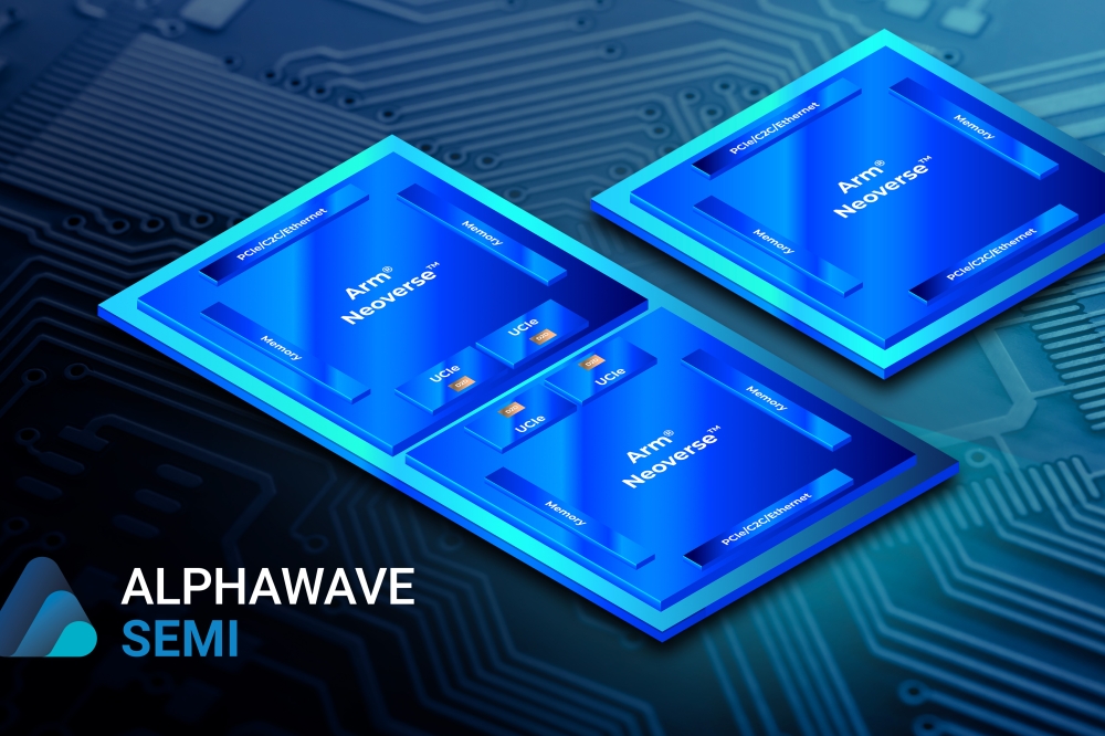
Alphawave Semi, a global leader in high-speed connectivity and compute silicon for the world’s technology infrastructure, has collaborated with Arm on the development of an advanced compute chiplet built on Arm® Neoverse™ Compute Subsystems (CSS) for artificial intelligence/machine learning (AI/ML), high-performance compute (HPC), data centre and 5G/6G networking infrastructure applications. The development follows last year’s announcement that Alphawave Semi joined Arm Total Design, an ecosystem building custom silicon solutions based on Arm Neoverse CSS.
Alphawave Semi’s chiplet-based custom silicon design platform adds a differentiator in our portfolio that includes IO extension chiplets, memory chiplets, and compute chiplets, as well as Alphawave Semi’s ultra-high-speed connectivity IP and advanced packaging capabilities. This compute chiplet lineup features an Arm Neoverse N3 CPU core cluster and the Arm Coherent Mesh Network (CMN) ensuring efficient, scalable performance. Available on industry-leading process nodes, the technology allows customers to accelerate development and reduce the time-to-market (TTM) of a new generation of custom system-on-chip (SoC) technologies. These advanced SoCs support the rapid deployment of high-performance digital infrastructure, enabling the creation of custom silicon solutions tailored to specific needs.
In collaboration with Arm, Alphawave Semi enhances this setup with their advanced packaging techniques and a leading-edge portfolio of connectivity technologies, including PCIe Gen 6.0 and 7.0, Universal Chiplet Express (UCIe), 112/224G Ethernet and HBM subsystems. This strategic integration ensures that the Arm-based compute chiplet delivers robust performance and flexibility, catering to next-generation HPC, data center, AI/ML, and 5G/6G infrastructure needs while accelerating time-to-market for customers.
“Our Arm-based compute chiplet is a critical component in Alphawave Semi’s custom silicon platform and a demonstration of both our IP, SoC and packaging capabilities and our successful strategic partnership with Arm,” says Mohit Gupta, Senior VP & GM, Custom Silicon & IP. Alphawave Semi. “Bringing together the Arm Neoverse CSS platform with Alphawave Semi’s advanced and proven IP drives innovation across the chiplet ecosystem and simplifies the development of critical custom silicon for AI, HPC and other demanding digital infrastructure applications.”
“Arm Total Design is fostering a rapidly growing ecosystem around custom silicon and enabling chiplet innovations to take on increasingly complex computing requirements,” said Eddie Ramirez, vice president of go-to-market, Infrastructure Line of Business, Arm. “Alphawave Semi’s new advanced compute chiplet is a fantastic example of how industry-leading companies are leveraging the performance-optimization and power efficiency benefits of Neoverse CSS to get to market faster and power the next-generation AI and HPC workloads.”


