VIS and NXP to establish fab JV

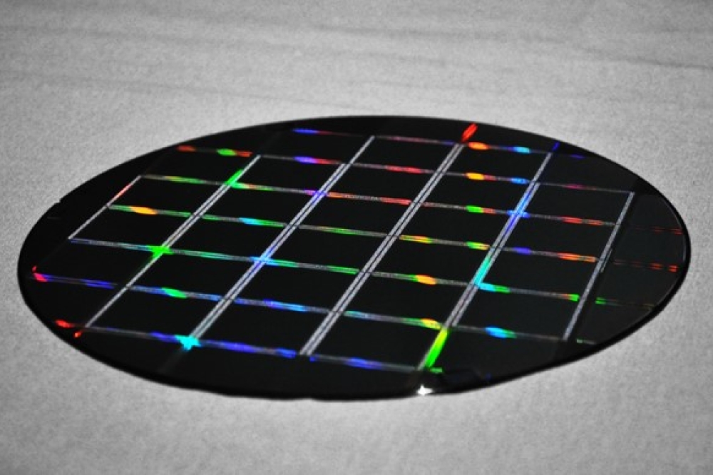
Vanguard International Semiconductor Corporation and NXP Semiconductors plan to create a manufacturing joint-venture VisionPower Semiconductor Manufacturing Company Pte Ltd (“VSMC”) which will build a new 300mm semiconductor wafer manufacturing facility in Singapore.
The joint-venture fab will support 130nm to 40nm mixed-signal, power management and analog products, targeting the automotive, industrial, consumer and mobile end markets. The underlying process technologies are planned to be licensed and transferred to the joint venture from TSMC.
The joint venture will begin construction of the initial phase of the wafer fab in the second half of 2024, pending receipt of all required regulatory approvals, with initial production available to customers during 2027. The joint venture will operate as an independent, commercial foundry supplier, providing assured proportional capacity to both equity partners, with an expected output of 55,000 300mm wafers per month in 2029. The joint venture will create approximately 1,500 jobs in Singapore. Upon the successful ramp of the initial phase, a second phase will be considered and developed pending commitments by both equity partners.
The total cost of the initial build out is anticipated to be $7.8 billion. VIS will inject $2.4 billion representing a 60 percent equity position in the joint venture and NXP will inject $1.6 billion for the remaining 40 percent equity position. VIS and NXP have agreed to contribute an additional $1.9 billion which will be utilized to support the long-term capacity infrastructure. The remaining funding including loans will be provided by third parties to the joint venture. The fab will be operated by VIS.
“VIS is pleased to work with leading global semiconductor company NXP to build our first 300mm fab. This project aligns with our long-term development strategies, demonstrating VIS’ commitment to meeting customer demands, and diversifying our manufacturing capabilities,” said VIS Chairman Leuh Fang. “Adhering to the vision of business sustainability, this fab will be built adopting the Singapore Green Mark standards and implementing rigorous green manufacturing measures. We will continue to create great value for our stakeholders and look forward to working with customers, suppliers, local talents, and government to continuously contribute to Singapore and the global semiconductor ecosystem.”
“NXP continues to take proactive actions to ensure it has a manufacturing base which provides competitive cost, supply control, and geographic resilience to support our long-term growth objectives,” said Kurt Sievers, NXP President and CEO. “We believe VIS is well suited and fully understands the complexities involved in building and operating together with NXP a 300mm analog mixed signal fab. The joint venture partnership we intend to create with VIS perfectly aligns within NXP’s hybrid manufacturing strategy.”


