
Fractilia has introduced FAME OPC for improved OPC modeling
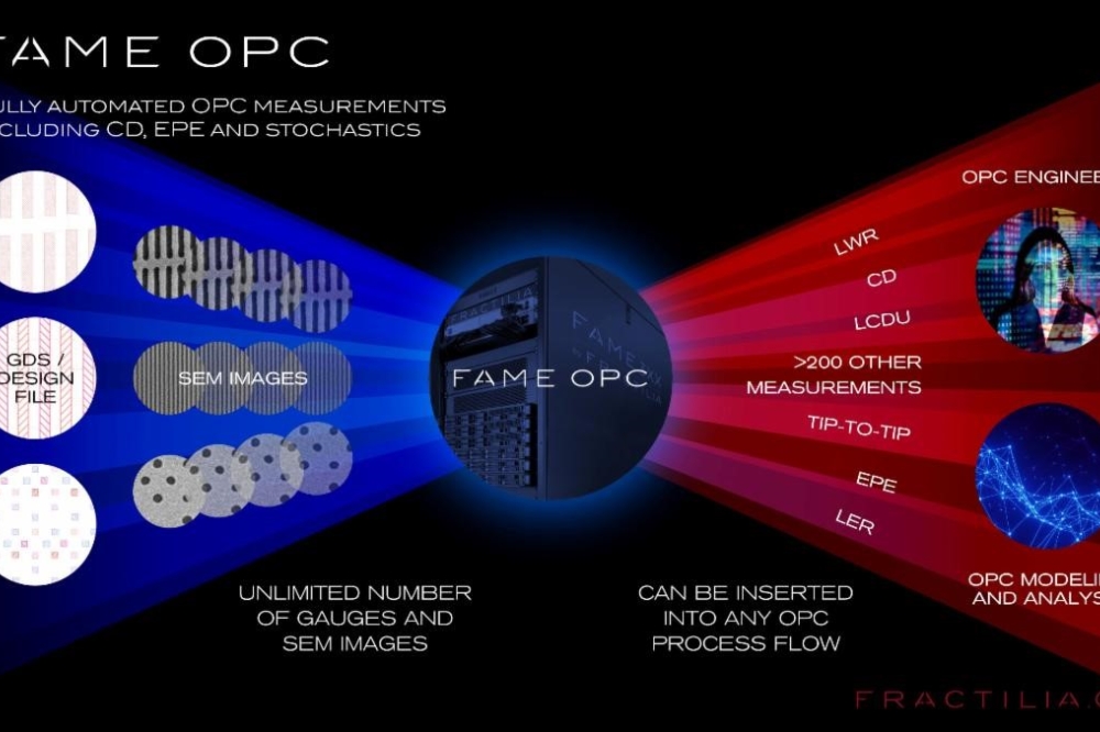
Fractilia, provider of stochastics metrology and control solutions for advanced semiconductor manufacturing, has introduced FAME OPC, a new product that provides critical optical proximity correction (OPC) measurement and analysis capabilities for improved OPC modeling – an essential technique used in advanced patterning. FAME OPC works with any SEM tool from any SEM vendor, can be inserted into any OPC data flow, and is available as a stand-alone product or as an add-on to customers’ existing Fractilia installed frameworks.
Fractilia’s FAME and MetroLER products, which combine the company’s patented Fractilia Inverse Linescan Model (FILM) technology with true computational metrology, are the only proven fab solutions that provide highly accurate and precise measurements of all major stochastic effects – the single largest source of patterning errors at advanced nodes. Fractilia is currently engaged with leading chip manufacturers in measuring and analyzing their OPC data with its new FAME OPC product.
CD Measurements No Longer Enough for OPC Model Verification
OPC is a patterning enhancement technique in semiconductor manufacturing that makes use of tiny edge deviations and sub-resolution assist features on the photomask to improve the printability of the desired chip pattern on the wafer. Each OPC model is calibrated using up to tens of thousands of features, called gauges, which if not measured with accuracy and precision can negatively impact process windows and yields. To calibrate the OPC models, chip manufacturers print wafers from a test mask and then measure the difference between how the gauges have printed compared to their design. In the past, customers would measure only the critical dimension (CD) and then incorporate these measurements into the OPC models for calibration of the models.
However, as chip feature sizes continue to shrink and as stochastic variability has increased with the adoption of EUV patterning, CD measurements are no longer enough for OPC model calibration and validation. Line-edge and linewidth roughness (LER/LWR), local edge-placement error (LEPE) and local CD uniformity (LCDU) as well as CD measurements must all be considered. The risk of stochastic variability is expected to only increase with the anticipated migration to high-NA EUV (0.55 NA EUV) lithography at the 2-nm node and beyond.
“For years, leading chip manufacturers have been using our MetroLER product to support their OPC model development and validation,” stated Edward Charrier, CEO and president of Fractilia. “While this has provided them with essential information to improve their OPC models, users have needed to manually perform the setup, measurement and analysis – a process that could take days to complete. Based on customer requests, Fractilia has developed FAME OPC, which fully automates the OPC measurement and analysis process. This enables our customers to measure CD and other distance measurements as well as hundreds of stochastic measurements from thousands of different gauges in as little as one hour, which significantly improves the accuracy and time-to-results of their OPC models.”
“Unbiased” Measurements Provide More Accurate Description of What’s on the Wafer
Fractilia’s FAME portfolio of solutions uses a proprietary and unique physics-based SEM modeling and data analysis approach that measures and subtracts the random and systematic errors from SEM images to provide measurements of what is on the wafer rather than what is on the images. FAME measures all major stochastic effects simultaneously, including LER, LWR, LCDU, LEPE, and stochastic defects, as well as provides CD and other distance measurements. It provides the highest signal-to-noise edge detection in the industry (up to 5X higher signal-to-noise ratio than other solutions), and extracts more than 30X more data from each SEM image. FAME works with SEM images from any SEM tool from and SEM vendor.
With FAME OPC, Fractilia brings the highly accurate measurement and analysis capabilities of FAME to OPC modeling. Users create a “master sheet” of all the measured gauges and then submit the job to FAME OPC along with all the SEM images and the design pattern such as a GDS/OASIS file. FAME OPC then automatically calibrates CD measurements to the SEM tool measurements, generates each Fractilia “recipe” file, measures the appropriate SEM images for each gauge and then combines the results for expedited analysis with the most accurate measurements available. By making this a fully automated process, FAME OPC significantly shortens engineering workload, and reduces time to results to determine the optimized OPC treatment by orders of magnitude.
Fractilia’s products have been adopted throughout the industry by dozens of companies, including leading semiconductor manufacturers, equipment companies, materials suppliers and research organizations. Improved lithography, etch and SEM tool matching, throughput, and overall equipment efficiency, as well as process window optimization, reduced cost of ownership and lower capital tool expenditures, are among the many benefits that can be achieved using Fractilia’s FAME and MetroLER products.


