EV Group and Fraunhofer IZM-ASSID expand partnership
Strategic partnership kicks off with installation of EVG850 automated laser debonding system at the newly launched Center for Advanced CMOS and Heterointegration Saxony (CEASAX).
EV Group (EVG) and Fraunhofer IZM-ASSID (All Silicon System Integration Dresden), a division of Fraunhofer IZM, have entered into a strategic partnership to develop and optimize alternative bonding and debonding technologies for advanced CMOS and heterogeneous integration applications, including quantum computing.
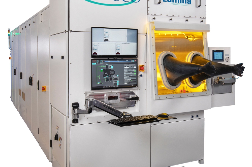
Kicking off this expanded collaboration, Fraunhofer IZM-ASSID has purchased and installed an EVG®850 DB fully automated UV laser debonding and cleaning system at Fraunhofer’s newly established Center for Advanced CMOS and Heterointegration Saxony (CEASAX), located in Dresden, Germany. CEASAX combines core competencies from Fraunhofer IZM-ASSID and the Fraunhofer Institute for Photonic Microsystems (IPMS) to further research into 300-mm, 3D heterogeneous wafer-level system integration and front-end semiconductor integration processes for high-performance neuromorphic computing, cryo- and quantum technology.
The EVG850 DB is the first system to be installed at CEASAX, and will help enable Fraunhofer IZM-ASSID to close critical process gaps and offer technology modules for the manufacturing of quantum systems and their wafer-scale hardware environment based on a 300-mm cleanroom environment. The system’s installation also marks the start of Fraunhofer’s Bond-Hub, which will additionally comprise a multitude of leading-edge temporary as well as permanent wafer-to-wafer and die-to-wafer bonding systems.
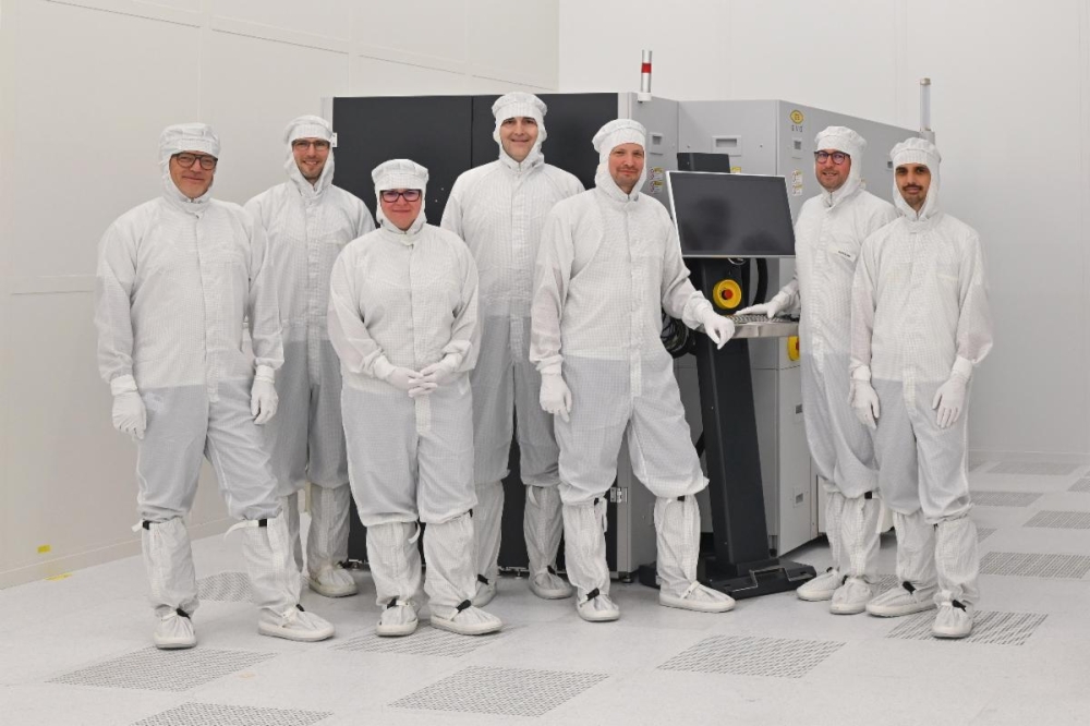
EV Group and Fraunhofer IZM-ASSID personnel next to an EVG®850 DB fully automated UV laser debonding and cleaning system installed in Fraunhofer’s newly established Center for Advanced CMOS and Heterointegration Saxony (CEASAX) in Dresden, Germany. From left to right: Gerald Silberer, Regional Sales Director Europe (EV Group); Dr. Andreas Gang, Group Leader Pre-Assembly / Wafer Bonding (Fraunhofer IZM-ASSID); Dr. Manuela Junghähnel, Site Manager (Fraunhofer IZM-ASSID); Markus Wimplinger, Corporate Technology Development & IP Director (EV Group); Andreas Pichler, Regional Sales Manager Europe (EV Group); Robert Wendling, Technical Assistant Wafer Bonding (Fraunhofer IZM-ASSID); and Dr. Frank Windrich, Deputy Site Manager (Fraunhofer IZM-ASSID). © Fraunhofer IZM / Silvia Wolf. Print quality: https://www.evgroup.com/company/news.
Temporary Bonding Essential for Heterogeneous Integration Applications
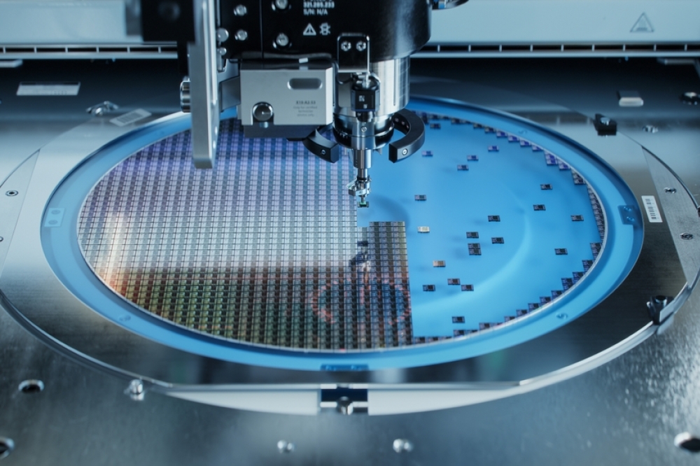
Temporary wafer bonding is a widely used method to ensure the processing of thin wafers (under 100-micron silicon thickness), which are important for 3D ICs, power devices and fan-out wafer-level packaging (FOWLP), as well as for handling fragile substrates like compound semiconductors. The debonding of the carrier wafer is an essential step to prepare the device wafer for the final process steps toward singulation and integration of the dies into the end device or application. By acquiring the EVG850 DB system, Fraunhofer can perform these debonding processes entirely in house, enabling significantly shorter development times for optimal process flows with various bonding adhesive systems. This in turn will allow Fraunhofer to ideally tailor its processes to the unique and specific needs of its many customers.
“Fraunhofer and EV Group have enjoyed a long and successful collaboration in developing new processes that have helped enable critical, emerging micro-electronics applications – including multi-device integration of analog and digital devices such as ASICs, RF devices, sensors and transceivers into an optimized system-in-package or functional smart microelectronic systems,” stated Manuela Junghähnel, site manager, Fraunhofer IZM-ASSID. “We are excited to be expanding and reinforcing this partnership through the purchase of the EVG850 DB laser debonding and cleaning system, which will be the first of several key product installations at CEASAX, our new advanced semiconductor research center. Through this expanded relationship, Fraunhofer will receive state-of-the-art technology in-house and have a strong partner in EV Group for developing new technologies for 3D device integration, which in turn will offer our customers a more complete process chain for 3D/heterogeneous integration from a single source.”
According to Markus Wimplinger, corporate technology development and IP director at EV Group, “We are excited to be building upon our long-term partnership with Fraunhofer into quantum computing applications and beyond through this latest strategic development. Our expanded collaboration allows EVG to stay at the forefront of technology advancements and enable us to contribute to the development of new manufacturing processes for quantum systems.”
EVG Heterogeneous Integration Solutions
EVG’s wafer bonding, lithography and metrology solutions enable the development and high-volume manufacturing of technology innovations in advanced packaging—including backside illuminated CMOS image sensors and other 3D-IC stacked devices—as well as in MEMS and compound semiconductors. Recent breakthroughs in hybrid bonding to address the needs for 3D device integration, wafer bond alignment technology to address future 3D-IC packaging requirements, IR laser release technology to eliminate glass substrates for advanced packaging and enable thin-layer 3D stacking, maskless exposure for fan-out wafer level packaging (FOWLP), and NIL and resist processing to support wafer-level optics (WLO) manufacturing, are just a few examples of EVG’s technology leadership in heterogeneous integration and wafer-level packaging.