Marvell introduces 'breakthrough' custom HBM compute architecture

New Marvell AI accelerator (XPU) architecture enables up to 25% more compute, 33% greater memory while improving power efficiency.
Marvell Technology has pioneered a new custom HBM compute architecture that enables XPUs to achieve greater compute and memory density. The new technology is available to all of its custom silicon customers to improve the performance, efficiency and TCO of their custom XPUs. Marvell is collaborating with its cloud customers and leading HBM manufacturers, Micron, Samsung Electronics, and SK hynix to define and develop custom HBM solutions for next-generation XPUs.
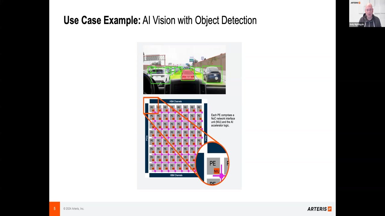
HBM is a critical component integrated within the XPU using advanced 2.5D packaging technology and high-speed industry-standard interfaces. However, the scaling of XPUs is limited by the current standard interface-based architecture. The new Marvell custom HBM compute architecture introduces tailored interfaces to optimize performance, power, die size, and cost for specific XPU designs. This approach considers the compute silicon, HBM stacks, and packaging. By customizing the HBM memory subsystem, including the stack itself, Marvell is advancing customization in cloud data center infrastructure. Marvell is collaborating with major HBM makers to implement this new architecture and meet cloud data center operators’ needs.
The Marvell custom HBM compute architecture enhances XPUs by serializing and speeding up the I/O interfaces between its internal AI compute accelerator silicon dies and the HBM base dies. This results in greater performance and up to 70% lower interface power compared to standard HBM interfaces. The optimized interfaces also reduce the required silicon real estate in each die, allowing HBM support logic to be integrated onto the base die. These real-estate savings, up to 25%, can be used to enhance compute capabilities, add new features, and support up to 33% more HBM stacks, increasing memory capacity per XPU. These improvements boost XPU performance and power efficiency while lowering TCO for cloud operators.
“The leading cloud data center operators have scaled with custom infrastructure. Enhancing XPUs by tailoring HBM for specific performance, power, and total cost of ownership is the latest step in a new paradigm in the way AI accelerators are designed and delivered,” said Will Chu, Senior Vice President and General Manager of the Custom, Compute and Storage Group at Marvell. “We’re very grateful to work with leading memory designers to accelerate this revolution and, help cloud data center operators continue to scale their XPUs and infrastructure for the AI era.”
“Increased memory capacity and bandwidth will help cloud operators efficiently scale their infrastructure for the AI era,” said Raj Narasimhan, senior vice president and general manager of Micron’s Compute and Networking Business Unit. “Strategic collaborations focused on power efficiency, such as the one we have with Marvell, will build on Micron’s industry-leading HBM power specs, and provide hyperscalers with a robust platform to deliver the capabilities and optimal performance required to scale AI.”
“Optimizing HBM for specific XPUs and software environments will greatly improve the performance of cloud operators’ infrastructure and ensure efficient power use,” said Harry Yoon, corporate executive vice president of Samsung Electronics and head of Americas products and solutions planning. “The advancement of AI depends on such focused efforts. We look forward to collaborating with Marvell, a leader in custom compute silicon innovation.”
“By collaborating with Marvell, we can help our customers produce a more optimized solution for their workloads and infrastructure,” said Sunny Kang, VP of DRAM Technology, SK hynix America. “As one of the leading pioneers of HBM, we look forward to shaping this next evolutionary stage for the technology.”
“Custom XPUs deliver superior performance and performance per watt compared to merchant, general-purpose solutions for specific, cloud-unique workloads,” said Patrick Moorhead, CEO and Founder of Moor Insights & Strategy. “Marvell, already a player in custom compute silicon, is already delivering tailored solutions to leading cloud companies. Their latest custom compute HBM architecture platform provides an additional lever to enhance the TCO for custom silicon. Through strategic collaboration with leading memory makers, Marvell is poised to empower cloud operators in scaling their XPUs and accelerated infrastructure, thereby paving the way for them to enable the future of AI.”

