
Flip chip technology market to reach $45.22 billion in 2032
The forecast period anticipates a substantial growth in the Global Flip Chip Technology Market.
Flip chip technology denotes the mounting of a semiconductor device or chip directly onto the circuit board, as opposed to conventional wire bonding methods. This innovative approach offers several benefits, including enhanced electrical performance, increased input/output density, and improved thermal management capabilities. The market's significance is underscored by its capacity to serve various sectors such as consumer electronics, automotive, telecommunications, and healthcare. The market's expansion is propelled by the escalating demand for smaller and faster electronic gadgets, coupled with the widespread adoption of advanced packaging technologies. Furthermore, the increasing requirement for compact and lightweight electronic devices is amplifying the need for flip chip technology. Nevertheless, the market's growth may be impeded by the high implementation costs and the challenges in ensuring reliable interconnections between the chip and the substrate. Despite these obstacles, the ongoing technological progressions and augmented investments in research and development are poised to unlock rewarding opportunities in the global flip chip technology market.
The market size for flip chip technology was estimated to be USD 27.02 billion in 2022. With a compound annual growth rate (CAGR) of 7.30% for the projection period (2023 - 2032), the flip chip technology market is expected to increase from USD 28.56 billion in 2023 to USD 45.22 billion by 2032.
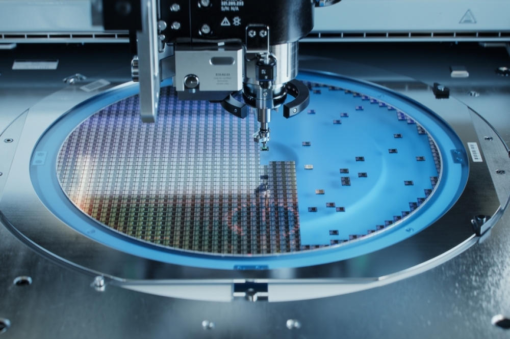
Flip Chip technology represents an advanced approach to integrated circuit packaging, offering a host of advantages in terms of performance, compactness, and dependability. In this innovative method, the silicon chip is affixed in a face-down orientation directly onto the substrate, facilitating immediate electrical connections between the two components. The electrical links are established through minuscule bumps made of solder or other conductive materials, commonly referred to as "flip chips." This methodology enables a greater concentration of connections, shorter signal pathways, and improved heat dissipation in comparison to conventional packaging techniques. By doing away with wire bonds and maximizing the chip's entire surface area, Flip Chip technology enhances electrical functionality and supports the creation of smaller, more efficient electronic devices.
Extensive research indicates that the Asia Pacific region is poised to emerge as the primary driver of the worldwide flip chip technology sector. This trend can be ascribed to the burgeoning expansion of the semiconductor realm in nations such as China, Taiwan, and South Korea. Furthermore, the region boasts a strong foothold of leading industry participants and a rising influx of capital into cutting-edge packaging technologies.
The primary technique anticipated to take the lead in the Global Flip Chip Technology market among wafer bumping processes is the CU Pillar method, surpassing Lead -free. The preference for CU Pillar technology stems from its ability to provide superior electrical conductivity and thermal performance. It also enables a reduction in pitch and enhances signal integrity, making it a suitable choice for cutting-edge packaging applications across industries such as automotive, consumer electronics, and telecommunications. Consequently, the CU Pillar process is expected to secure a dominant position in the Global Flip Chip Technology market.
Furthermore, the 2.5D packaging technology is poised to dominate the Global Flip Chip Technology market by offering a cost-effective alternative to 3D packaging without compromising on performance when compared to conventional 2D packaging solutions. This advanced packaging technique allows for vertica l stacking of multiple chips, leading to enhanced thermal management and superior electrical performance. Its widespread adoption in diverse applications like smartphones, gaming devices, and automotive electronics further solidifies its prominence in the market. Ultimately, the 2.5D packaging technology strikes a favorable balance between performance, cost-effectiveness, and broad applicability, positioning it as the preferred choice in the Global Flip Chip Technology market.


