
Imec unveils CMOS-based 56Gb/s zero-IF D-band beamforming transmitter
Designed to support next-generation, short-range, high-speed wireless services at frequencies above 100GHz – from wireless fail-safes in data centers to extended reality (XR) solutions.
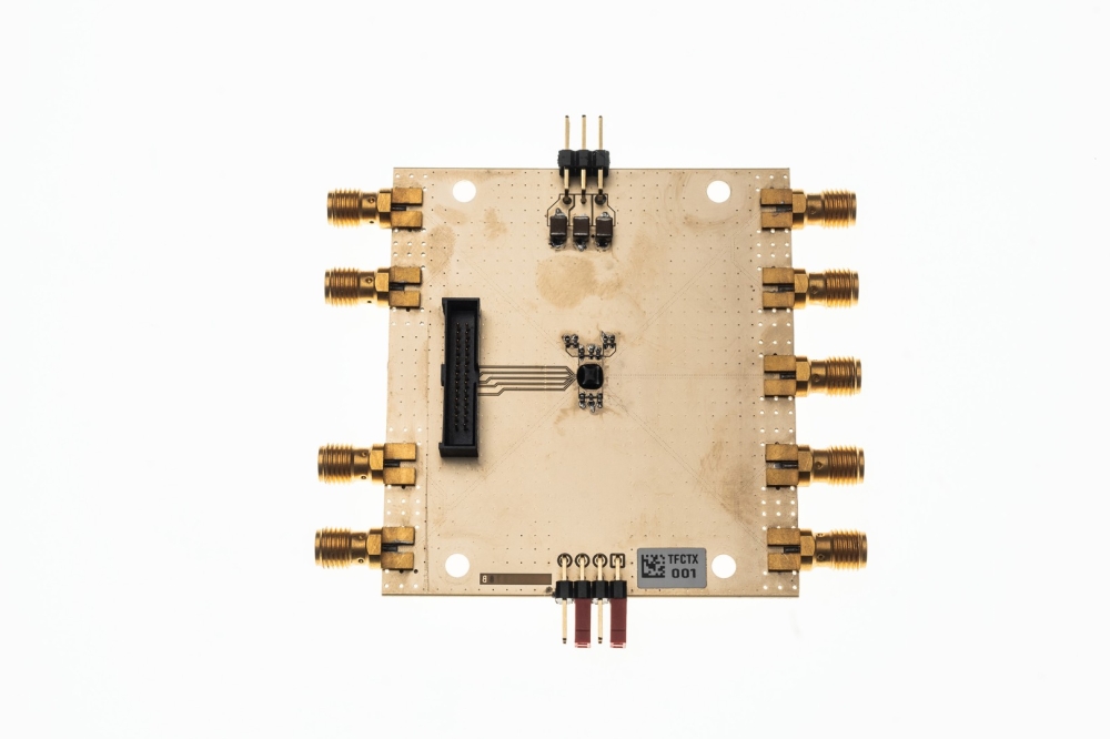
At this week’s IEEE RFIC Symposium, imec presents a state-of-the-art CMOS-based beamforming transmitter for D-band wireless applications. The transmitter features exceptional output power and energy efficiency while supporting data rates of up to 56Gb/s per channel. It is a key component of a 4-way beamforming transceiver chip currently being developed by imec’s researchers. With this technology, they aim to support the deployment of next-generation, short-range wireless services at frequencies above 100GHz.
Next-generation short-range wireless applications, boasting data rates in the tens of gigabits per second, usher in an era of opportunity. Whether it's data centers in search of wireless fail-safe mechanisms, fixed wireless access (FWA) deployments, or wireless hotspots enabling extended reality (XR) experiences, they are all converging on the sub-THz bands between 100 and 300GHz.
The ample bandwidth offered by these frequencies is just one of the essential features. In addition, their shorter wavelengths allow for smaller antennas, enabling increasingly compact access points and handheld devices. Finally, the high sensing resolution will prove invaluable in future applications (gaming, smart buildings, Industry 5.0, ...) where communication and sensing are intertwined.
“Yet, when CMOS technology ventures into the realm of 100GHz and beyond, it encounters various obstacles. The first challenge is to achieve sufficient output power to overcome the higher pathloss at these frequencies. It’s also much more difficult to realize wideband circuitry with good dynamic range and acceptable power consumption. These challenges are at the heart of our novel CMOS-based D-band beamforming transmitter,” explained Joris Van Driessche, program manager at imec.
A high data rate, low power CMOS-based D-band beamforming transmitter
Imec’s transmitter, part of a 4-way beamforming transceiver architecture, operates in the 120-145GHz frequency range. Designed using a 22nm FD-SOI process, each transmitter channel occupies an area of 1.17x0.3mm² and consumes 232mW of power. And with a Pout of 3dBm for 16QAM modulation and 2dBm for 64QAM modulation, imec’s implementation stands out as a top performer among CMOS D-band transceivers in terms of transmitted output power.
By implementing beamforming in the local oscillator circuit to steer high-gain narrow beams in specific directions, in combination with a zero-IF transceiver architecture, imec's transmitter reduces the number of components in the signal path. As such, the dynamic range of the signal path is preserved, and a wide RF bandwidth can be achieved. In addition, imec's design features a wideband analog baseband section covering channel bandwidths up to 14GHz, enabling high data rates (up to 56Gb/s per channel) across a broad frequency range.
Joris Van Driessche: “And yet another unique feature of our chip is its completeness. Unlike competing solutions, ours seamlessly integrates LO beamforming and a full analog baseband section across all four channels, along with the complete RF chain and beamforming functionality. To our knowledge, this is a significant first.”
Inviting partners to explore the technology’s potential
“The paper presented at the IEEE RFIC Symposium focuses on the results we’ve achieved with our new beamforming transmitter. However, our research has since led to the development of a complete 4-way beamforming transceiver chip, which is currently undergoing further characterization. With this chip, we aim to build a D-band wireless system that will allow partners to experiment with beamforming technology, joint communication and sensing (JC&S) applications, and more – while demonstrating the viability of CMOS technology for next-generation, short-range wireless applications at frequencies above 100GHz,” concluded Van Driessche.
This research is part of imec’s Advanced RF program, which aims to enable next-generation, high-data-rate wireless and high-resolution sensing applications by addressing challenges from the device level, up to the system level.


