
OMNIVISION introduces 'smallest camera module'
New OCH2B30 CameraCubeChip® module is a compact wafer-level module with superior video quality.
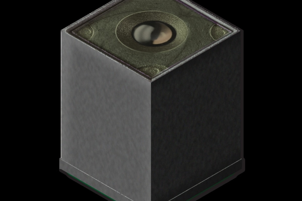
OMNIVISION has introduced the new OCH2B30 camera module for three-dimensional (3D) intraoral dental scanners. The OCH2B30 features a compact CameraCubeChip® package in an ultra-small form factor (2.6 mm x 2.6 mm) with exceedingly high image quality and MIPI interface for cameras in benchtop, standalone and portable intraoral scanners.
“Intraoral scanners are quickly replacing the use of traditional dental impression in dentistry today. We are leveraging our proven technology from the medical endoscopy market to help advance intraoral scanners for dentistry,” said Aaron Chiang, marketing director, OMNIVISION. “Our CameraCubeChip® technology enables the smallest camera modules for 3D intraoral dental scanners. Similar in size to the actual CMOS image sensor inside the camera, the CameraCubeChip® enables ultra-compact, high-resolution cameras, which is especially important when there are multiple cameras in each scanning device. We expect the new OCH2B30 camera module to play an important role in driving the growth of the intraoral dental scanner market and, ultimately, in improving patient care.”
The global dental intraoral scanner market is growing with a compound annual growth rate (CAGR) of 11.1% in the forecast period of 2023 to 2030 and is expected to reach USD 1,325.80 million by 2030 from USD 573.76 million in 2022.1 This growth is being driven by the increasing demand for cosmetic dentistry, the prevalence of dental diseases and new technological advancements in dentistry. Intraoral scanners are used primarily by orthodontists, endodontists, periodontists, prosthodontists and general dentists.
The OCH2B30 camera module has a 2-megapixel (MP) resolution square-format CMOS image sensor with a 1.12-micron (µm) pixel built on OMNIVISION’s latest PureCel®Plus-S stacked-die technology, which enables its ultra-small size. At 1500 x 1500 resolution, the OCH2B30 achieves 60 frames per second (fps), and at 720p resolution, 120 fps.
Medical Certifications Streamline FDA Approval Process
OMNIVISION is ISO13485-certified. The OCH2B30 is tested for EMC/EMI compliance and sterilization, and it is biocompatible and waterproof. Because it passes OMNIVISION’s rigorous production testing, it is guaranteed to be within the stated electrical, mechanical and optimal specifications, and hence does not require tuning or calibration.


