Silicon’s dual role: Fueling AI’s need for computation and connectivity

By Alan Keizer, Senior Technology Advisor, AFL
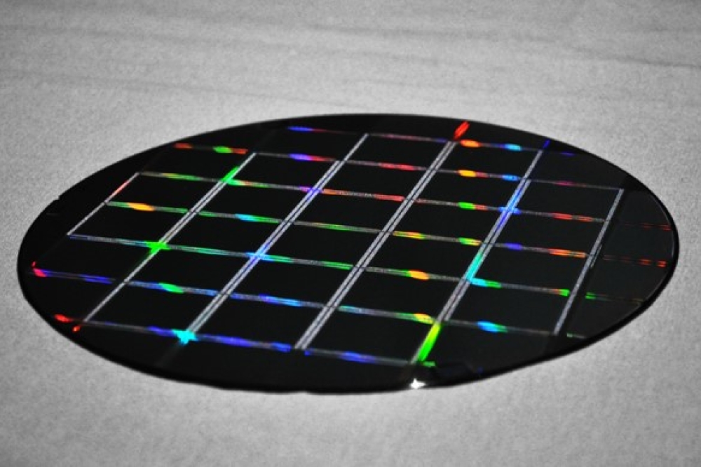
Silicon is the basic building block of hyperscale technology. Pure silicon is highly reactive and, in nature, always combines with other elements – most commonly oxygen to form silicon dioxide (SiO2), or silica, the material used in the construction of almost all optical fiber. Given their mutual material makeup, optical fibers and silicon semiconductors share similar timelines for innovation, miniaturization, and enhanced performance.
Co-design describes the collaborative approach to innovation across optical fibers and the system architectures configured for entire optical networks. More simply, performance optimization is made easier where the components and systems set up to improve scalability, efficiency, and resiliency undergo complementary refinements, benefitting the real-world applications of the dual technologies.
AI model training requires massive computational power (compute). AI’s insatiable appetite for compute resources dwarves traditional computing workloads. The generative AI boom’s growing need for seamless data processing ties R&D directly to silica optical fiber and silicon semiconductors.
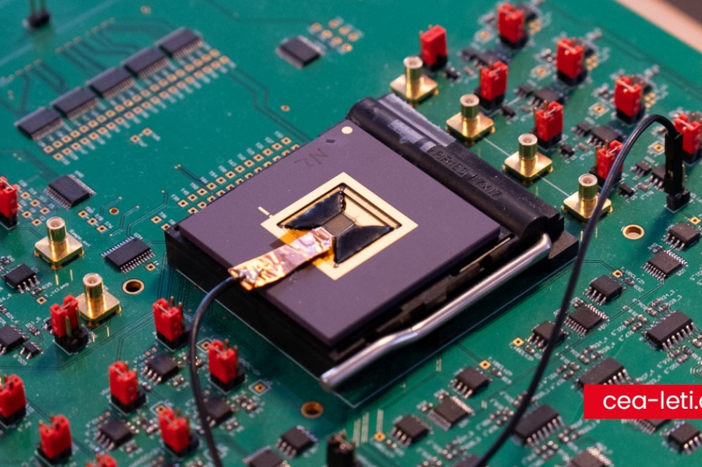
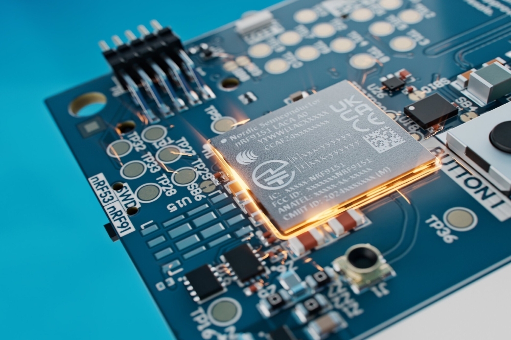
Silicon’s characteristic ability to selectively conduct electricity under controlled conditions makes it the preferred material for transistor fabrication – not only does AI connectivity rely upon advancements in silicon-based technologies, but advancements in the transistor world of switching, amplification, and digital logic operations also depends heavily upon miniaturized silicon structures to increase the transistors-per-microchip count. However, resolving the challenge evokes Moore’s law.
Shrinking transistors and Moore’s Law
In 1965, Gordon Earle Moore (co-founder of Fairchild Semiconductor and Intel) noted the predictable relationship between time passing and transistors per integrated circuit. Initially, Moore’s observation stated transistor counts for microprocessors would double each year. In 1975, Moore revised this guidance, predicting the doubling in number of integrated circuit transistors every two years.
Interestingly, Moore’s Law became an industry roadmap for long-term innovation, acting as a self-fulfilling prophecy for setting and realizing timeframes in technological advancement. Throughout the 1990s, Moore’s Law settled on a doubling period of 18-24 months.
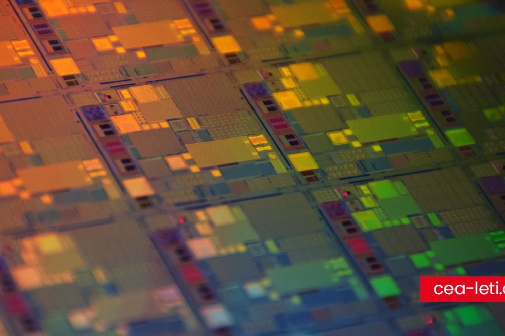
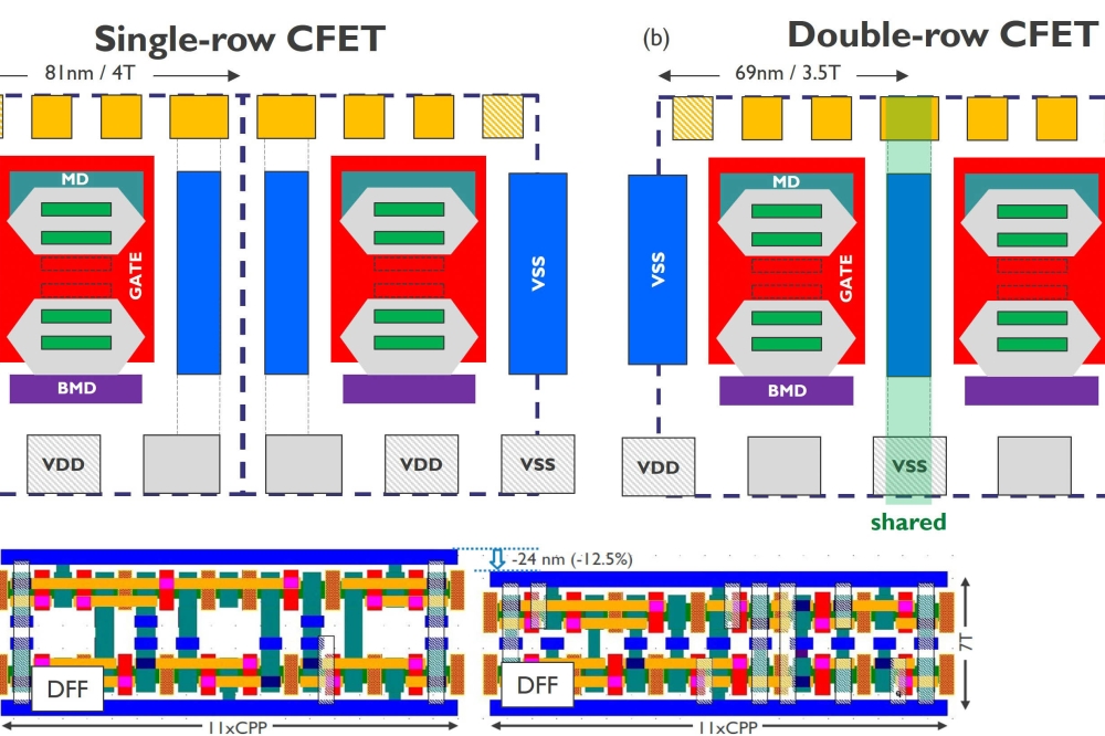
Lithographic advancements have given rise to precision component etching at the transistor component manufacture stage, enabling transistors to keep pace with Moore’s Law. By steadily developing the process, modern lithography enables manufacturers to shrink transistor dimensions and improve performance. Over the decades, creative three-dimensional design and high layer count have greatly contributed to higher density and lower power per unit of performance.
Let’s take a closer look at real-world examples of chips with billions of transistors, progressing over time:
1971 - Intel 4004: ~2,300 transistors, 10-micron process.
1995 - Intel Pentium Pro: ~5.5 million transistors, 350-nanometer process.
2020 - AMD Ryzen Threadripper 3990X: ~39 billion transistors, 7-nanometer process.
2024 - The Extreme Ultraviolet Lithography system from ASML delivers 2nm features. Nvidia introduces the B100 accelerator with over 100 billion transistors based on 2nm technology.
The limitations and challenges in continuing this miniaturization trend indefinitely lie not only with the obvious physical boundary of silicon atomic size, but also in cooling – increasing component count in a decreased space brings considerable heat dissipation challenges, requiring research and investment into sophisticated cooling technologies.
At the atomic level (where single digit nanometer technology is headed), the unpredictable presence of small dimensions can result in quantum tunneling, which when controlled is central to transistor operation but can have undesired outcomes when not intended. Quantum tunneling dictates that the atomic-scale proximity of components will see signal interference through uncontrolled electron sharing, rendering the processor ineffective.
Harnessing light at a miniature scale
The principle of total internal reflection underpins optical fiber technology. This phenomenon only occurs where the angle is shallow, much like skimming a stone on still water.
Innovations such as core-cladding and doping further enhance fiber’s transmission of relatively lossless light signals. Utilizing the principle of total internal reflection, a less dense material forms the cladding around the denser fiber. Doping is used to control the numerical index of refraction (N) to create higher or lower N materials from which to fabricate the core and cladding elements of single mode fiber. The core typically has a slightly higher N than the cladding. Doping involves adding elements to both the cladding and fiber core, optimizing performance (especially over long distance). Specialized fiber types and doping techniques help to minimize signal loss. Optical fiber transmission speeds have increased from Mb/s to hundreds of Gb (and even Tb/s):
1980s: Commercial systems at 565 Mb/s were state-of-the-art.
2000s: 10 Gb/s links became standard for long- haul infrastructure.
2010s: Coherent transmission techniques enabled 100 Gb/s and 400 Gb/s per fiber pair.
Today: Focus on terabit capacity per single fiber with advanced multiplexing and modulation.
Today, typical Single Mode Fiber (SMF) at 1550 nm wavelength has a loss of around 0.2 dB/km. Specialized Ultra-Low Loss fibers can achieve 0.15 dB/km or less, critical for extreme distances.
Wavelength-division multiplexing (WDM) multiplies fiber capacity. WDM can put 100+ wavelengths (colors) on a single fiber, each carrying tens or even hundreds of Gbps. Multiple colors of light can travel independently on the same fiber, significantly enhancing its bandwidth.
Optical components on silicon
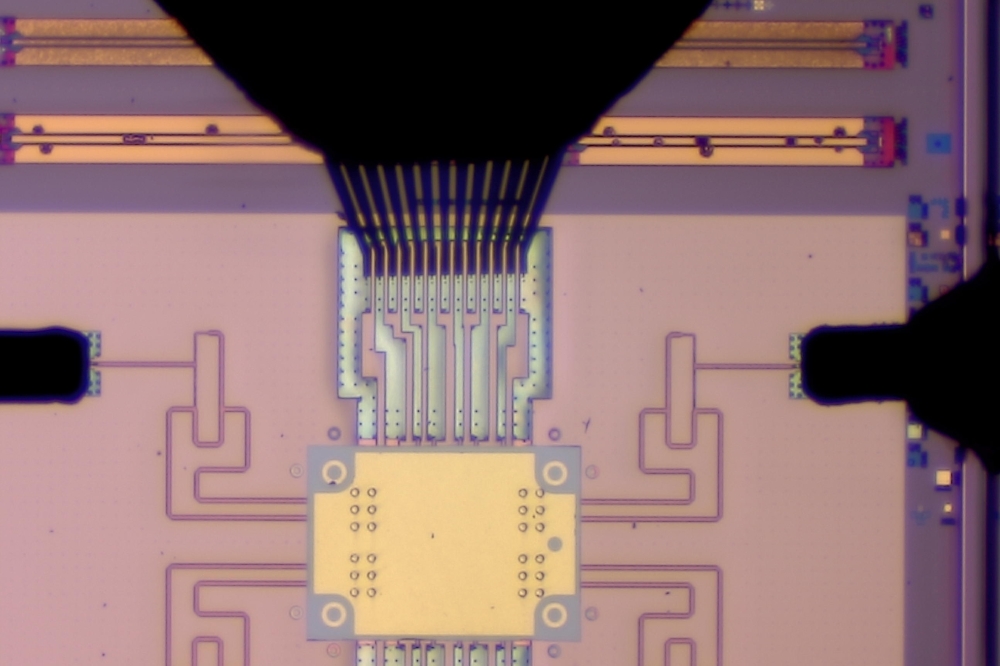
Advances in silicon photonics can help overcome the growing demand for high-speed connectivity. The technology enables electronic signal processing and light signal manipulation/transmission on the same chip. The reduced power consumption has applications across next-generation communication. Modern silicon photonic transceivers can achieve upwards of 1Tbps within a fingernail-sized package. The same manufacturing plants used for electronics can be adapted for silicon photonics, promising cost advantages.
Complementary Metal-Oxide-Semiconductor (CMOS) technology is the mainstay of integrated circuit construction. CMOS compatibility (e.g., high temperature threshold, using non-reactive materials such as silicon, and maintaining uniformity and performance when layering) is a consideration around optical waveguides, modulators, and detectors on silicon chips.
Electrical transmission on host printed circuit boards at very high data rates is limited in distance. 100G signals have a maximum transmission distance in high-performance circuit boards of 200mm or less.
Co-design: breaking boundaries for AI
Limitations in both semiconductor scalability and optical fiber capacity create system-level bottlenecks. Where the interconnect speed is not matched, even the fastest GPU can be starved for data. Training machine learning (ML) models across multiple machines is essential to achieve reasonable processing times, emphasizing chip-to-chip and node-to-node communication to achieve high performance.
To illustrate the issue, consider the limitation placed on nanosecond computations where electrical data movement between chips becomes a bottleneck for AI. Co-packaged optics (CPO) provide viable market solutions.
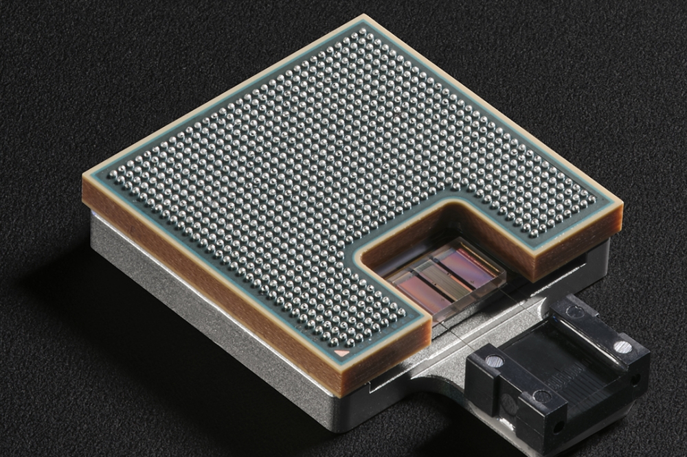
CPO integrates optical communication components and electronic semiconductor chips, reducing both latency and power consumption. By creating a single package incorporating silicon and optics with high capacity and low energy consumption, the potential emerges for wider industry applications. Also, as silicon is not the optimal choice for some electro-optical devices, a different semiconductor platform represents a significant advantage (e.g., gallium arsenide phosphide or other III/V or II/IV compounds).
Examples include:
Telecommunications – 6G Radio Access Networks (RANs)
CPO will accelerate innovation across signal processing, integrated circuit architectures, and optical communications and packaging, leading to the emergence of 6G RANs – this includes AI-enabled Radio Access Network, Aerial Radio Access Networks (ARANs), and Open Radio Access Networks (O-RANs). Through greater use of RANs and the terahertz (THz) spectrum, 6G could launch commercially by 2030.
Medical – quantum dot lasers
Co-packaged optics systems enable the compact, energy efficient performance necessary for quantum dot lasers. Commercially available but not yet widely adopted, quantum dot lasers use quantum dot semiconductor particles measured
in nanometers – much smaller than the bulk semiconductor material found in conventional lasers. Applications include precision laser surgery and tissue coagulation.
AI – training and inference
AI and machine learning require massive data processing and seamless data sharing between distributed computing systems. Integrating optical interconnects and packing more computing devices closer together can help reduce latency, enhance system performance, and accelerate data movement.
Hybrid switching brings together the benefits of both circuit and package switching to better accommodate diverse traffic (i.e., data centers can route latency-sensitive traffic such as video via circuit switching, whereas internet browsing can be routed via packet switching). Examples include:
Cloud networking
Hybrid switching enables greater connectivity between public cloud platforms and on-premises facilities.
Internet service providers (ISPs)
ISPs deploy hybrid switching to optimize service quality through networking resource allocation.
Data center networks
Data center hybrid switching may involve traditional core network ethernet switching for high-speed connectivity and network edge Software Defined Networking (SDN) switching for dynamic traffic management.
The holistic co-design approach breaks boundaries in support of AI system advances, resolving challenges across bandwidth, energy efficiency, and latency.
For example, instead of off-chip optical transceivers connected via electrical signals, silicon photonic chips could be placed directly next to AI processors, reducing the distance electrical signals must travel.
This reduced proximity is a consideration in electrical interconnect power consumption over various link distances. For example, consider a 100 Gbps link over 1 kilometer. In this scenario, electrical interconnects would consume a minimum of 20 Watts where optical interconnects would consume less than 10 Watts.
The future: beyond silicon’s limits
Co-design can help innovators to overcome the existing limitations of silicon. By incorporating emerging technologies, materials, and design ideas, co-design will revolutionize how we currently think about the inherent limitations of silicon-based solutions. Examples include:
III-V material integrations
Integrating silicon and elements from groups III and V in the periodic table to create semiconductor alloys can enhance carrier mobility, reduce power consumption, and enable previously unthinkable functionality.
Polymers and ceramics
Combining silicon with polymers and ceramics to create multi-functional, flexible, enhanced systems has potential commercial uses in bioelectronics and photonic integrated circuits. Wavelength splitters, comb filters, and modulators can be fabricated and integrated with waveguides to make compound optical devices.
Innovative design methodologies
Co-design facilitates technological integrations between silicon-based systems, enabling advanced modeling and simulation techniques used to enhance and optimize next-level manufacturability.
At this advanced stage, greater experimentation into wider materials – as mentioned above – is perhaps required to deliver on the promise of enhanced performance.
Conclusion
The journey from bulk silicon to sophisticated optical and computational components involves several complex stages, including wafer preparation, photolithography, and doping. The resulting high performance of silicon-based communication technologies pushes the limits of AI and connectivity.
Co-design between existing and new materials provides the logical next step in unlocking AI’s potential. The industry – and indeed the wider world – awaits further innovation regarding quantum communication and photonic neural networks.
As these emerging technologies continue to mature, their convergence will bring new levels of security and increased processing power, along with the kinds of crucial energy efficiency upgrades necessary to revolutionize and scale AI applications.
From a scientific curiosity to everyday life, AI and the innovations that power its continued onward march are undoubtedly here to stay. Silicon is the common element.


