
CEA-Leti presents complementary developments in 3D Integration Technologies
CEA-Leti scientists presented three papers at the IEEE Symposium on VLSI Technology and Circuits detailing the institute’s progress on 3D integration technologies, which are a promising approach for designing More than Moore systems, especially radio frequency (RF) integrated systems.
3D integration techniques enable high-density CMOS transistors to coexist with transistors made of III-V materials, which can reach power levels and frequencies unattainable with conventional silicon technologies. Potential applications include communications, the internet of things, medical devices and automotive sensing.
‘RF Performances Are Competitive with Other 3D Solutions’
The paper, “Hybrid Integration of 3D-RF Interconnects on AlGaN/GaN/Si HEMT RF Transistor featuring 2.2W/mm Psat & 41% PAE @28GHz using a Robust and Cost-Effective Chiplet Heterogeneous Bonding Technique”, reports the stacking of an AlGaN/GaN/Si high electron mobility transistor (HEMT) on coplanar-waveguide (CPW) lines fabricated on 200mm silicon trap-rich substrate. The HEMT and CPWs lines were interconnected with copper pillars (CuPi) using a high-yield chiplet heterogeneous integration process.
“Thanks to the integration of low insertion loss CuPi interconnects – 0.1dB@28GHz and a careful management of the heat dissipation within the 3D structure – the HEMT transistor features an output power density of 2.2W/mm @10V & a peak PAE of 41 percent,” the paper reports.
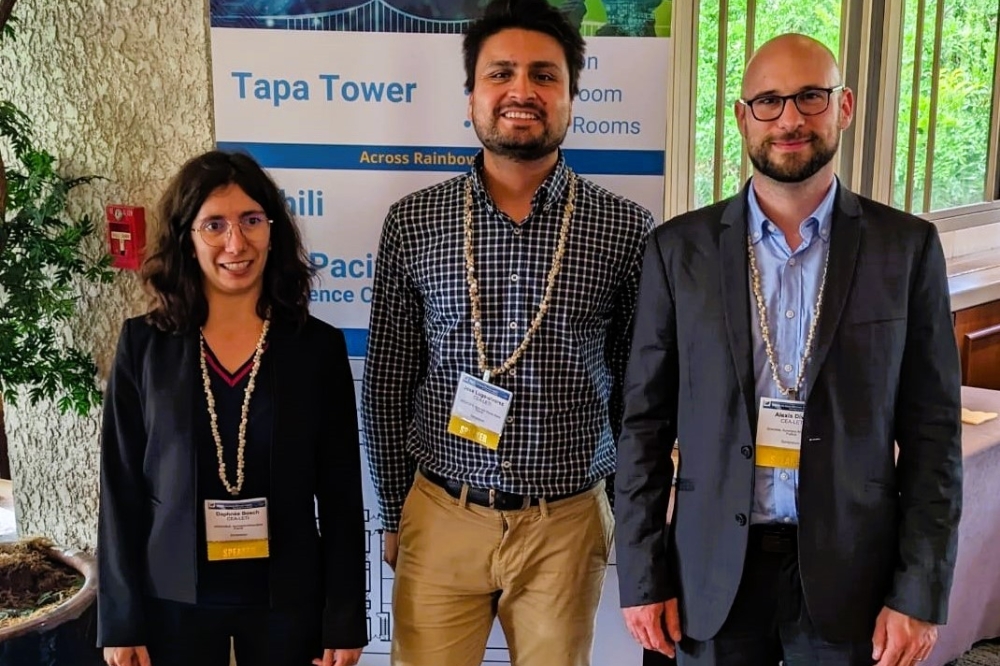
“These RF performances are competitive with other 3D solutions found in the literature,” said Alexis Divay, lead author of the paper. “Our industrial-grade 3D assembly approach is highly promising for fabricating efficient and cost-effective 3D-RF III-V systems.”
‘Results Lay the Groundwork for Using 3D Technologies to Enable RF Applications’
The paper, “First Radio-Frequency Circuits fabricated in top-tier of a full 3D Sequential Integration Process at mmW for 5G applications”, details how for the first time 5G-compatible (30GHz) RF circuits have been stacked directly above a working digital circuit. The analog silicon RF circuits, sequentially fabricated at 500°C above a digital circuit layer with a 28nm FD-SOI industrial platform, presented performance in line with standard, thermal-budget FD-SOI devices.
“Both top- and bottom-tier circuits are fully functional with good performance after the 3D-SI process,” said lead authors José Lugo and Jean-Baptiste David. “Moreover, we explored a worst-case scenario to assess potential detrimental impacts of the ultra-thin proximity between analog-RF circuits and the digital layer. The work demonstrated the feasibility of vertical co-integration without any degradation, despite the close vicinity of both tiers. These results lay the groundwork for using 3D technologies to enable to RF applications.”
‘CEA-Leti Creates a Path Toward a Second Step in 3D Silicon-Integration Development’
The paper, “Breakthrough processes for Si CMOS devices with BEOL compatibility for 3D sequential integrated More than Moore analog applications”, reports unlocking low-temperature “showstoppers” in versatile analog high-voltage (>2.5V) BEOL (400°C) devices.
“We demonstrated for the first time the nanosecond laser annealing, solid-phase epitaxial regrowth on a complete device, which surpasses the low-temperature, dopant activation technological showstopper,” said Daphnée Bosch, lead author of the paper.
The paper notes that the work also “demonstrated monocrystalline silicon devices with a CMOS-compatible poly gate thanks to nanosecond laser annealing in melt regime and junction dopants activation without diffusion at 400°C.” This preserves the engineered junction profile. “HPD2 final anneal cures low-temperature gate stack, achieving performances in line with planar analog CMOS technology.”
Co-author Perrine Batude said some of CEA-Leti’s industrial partners already have introduced a part of its vision: a second device layer integrated sequentially using monocrystalline channel bonding above a bottom device. However, the top pixel MOSFETs are currently processed at 1,000°C.
“With this paper, CEA-Leti creates a path toward a second step in 3D-silicon integration development with 400°C top devices stackable above a less resilient bottom tier,” she said.
Fourth Paper
A fourth paper presented by the institute at the conference covered “A Current-Source-Free Constant-Current Wireless Adiabatic Neural Stimulator Achieving a 5.5-27.7x Improved RF-to-Electrode Stimulation Efficiency Factor”.


