A sustainable semiconductor industry needs smarter water management

As the industry expands exponentially, so does its needs for water. Dan LeCloux, SVP of Research, Development, and Engineering for Ecolab’s Industrial division, says responding to growing demand responsibly requires companies to look at sustainability, water stewardship and productivity through a circular lens. While Mukul Girotra, vice president and general manager of Global High Tech for Nalco Water, an Ecolab company, shares his perspective on how manufacturers can use smart water management to balance sustainability, productivity and reliability in their operations.
SIS: Water stress is a growing issue worldwide. How does this impact semiconductor manufacturing, especially considering the water intensity of the industry?
DL: Manufacturers are facing significant and seemingly paradoxical challenges. On one hand, water stress remains a critical reality, with global freshwater demand projected to outpace supply by up to 56% by 2030 (according to the World Resources Institute). At the same time, the need for water in manufacturing continues to grow exponentially. The United Nations estimates demand will have increased by 400% between 2000 and 2050.
The microelectronics industry makes up a significant proportion of manufacturing water use, and many companies are actively seeking opportunities to reduce their water footprint. The industry is expected to grow by 6-8% every year through
2030, and its water requirements will scale accordingly.
Some semiconductor fabricators turn to air-cooled technologies as an alternative, but air-cooling requires substantial energy that results in increased greenhouse gas emissions – a significant trade-off. To build resilient, responsible operations, manufacturers need to look at water, climate and productivity together through a circular lens so they can minimize environmental impacts while maximizing production output and quality.
SIS: How would you characterize the complexity facing the microelectronics industry?
MG: Demand for smart phones, wearable devices and other technology continues to surge. Regional policies support expansion of the industry to meet demand, such as the CHIPS and Science Act legislation in the United States. At the same time, the semiconductor components that power this technology have gotten smaller – a trend driven by innovation in the industry. As a result, manufacturers must reconcile growing production requirements with increasingly elaborate processes as they work with reduced feature sizes.
Semiconductor fabricators also face pressure related to the water intensity of their operations. As an example, estimates suggest a single smart phone requires more than 3,000 gallons (11,300 liters) of water to produce. In response, many manufacturers are looking for circular strategies to manage and minimize water consumption while meeting their productivity goals.
SIS: How can a manufacturer evaluate their water intensity? What’s a practical first step?
DL: It starts with a plant assessment that results in a sustainability plan. Water use goes beyond linear treatment within the plant itself; it impacts the surrounding community. When conducting a plant assessment, semiconductor fabricators need to look inside and outside the facility fence to examine their water needs against available resources. Opportunities often exist to reduce, reuse, and recycle water from specific processes, or even from effluent sources, for utility applications, like cooling water make-up. By identifying these types of opportunities, manufacturers can build a smart water management approach that minimizes community strain and still prioritizes business objectives like yield, uptime and product quality.
SIS: What makes the water demands of semiconductor manufacturing unique when compared to other industries?
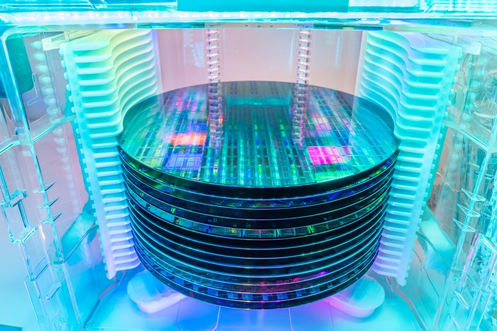
MG: As semiconductor components get smaller, the water requirements of manufacturing processes get more stringent. Fabricators rely on ultrapure water sources to produce semiconductors, and the quality of ultrapure water helps maintain the integrity of the delicate circuits on semiconductor wafers.
In addition to ultrapure water, semiconductor manufacturers also need to manage utility and wastewater operations like other industries. Cooling towers, chillers and boilers require treatment programs to minimize corrosion, scaling potential, and other risks, and wastewater streams can contain metals, fluoride and other contaminants that must be removed. Altogether, these water sources require a specialized approach — what we call ‘smart water management’ — to help semiconductor manufacturers minimize use, maximize quality, and reduce potential risks that could impact manufacturing assets.
SIS: Are there specific factors to consider when identifying water reuse opportunities?
DL: Recycling water requires an understanding of the composition of each available water source, as well as its end use. Different water sources require specialized forms of treatment to remove containments that can cause fouling, scale potential, or other risks. For example, effluent wastewater requires a treatment program that addresses the most critical components in the water stream, such as metals or fluoride. An optimized program can help a fabricator recycle and treat water to meet specific quality requirements, allowing them to reuse the water as utility make-up water in their operations.
To give a specific example of our work in this space, we helped a Texas-based manufacturer, NXP Semiconductor, reclaim water from its fabrication processes for use in the utility center’s cooling towers. We knew this solution would only work if we took steps to protect the assets from contaminants in the reclaimed water, such as phosphates, fluorides, sulfates, chlorides, ammonia and silica, as well as naturally occurring hardness caused by calcium and magnesium. These contaminants can increase corrosion, scale and other risks in the cooling water system.
By combining 3D TRASAR™ automation technology, Ecolab Global Intelligence Center monitoring and comprehensive on-site service, we delivered a real-time corrosion control solution that led to significant results. In a single year, the manufacturer saved 7.2 million gallons (27.2 million liters) of municipal water and reduced wastewater discharge by 8.5 million gallons (32.1 million liters).
SIS: Can you explain the smart water management concept? What does it entail?
MG: Smart water management looks at the water needs of a semiconductor manufacturer holistically. Our approach combines digital technology with innovative chemistry programs and institutional expertise to help companies address water use, productivity, and other sustainability levers — like energy and greenhouse gas emissions — all at once.
Digital solutions, like 3D TRASAR™ technology powered by the ECOLAB3D™ intelligence platform, can measure water system performance at the asset, site and enterprise level. With visibility to water consumption, quality conditions, and other insights, semiconductor manufacturers can keep a pulse on the health and reliability of their operations in real time. These solutions, in concert with innovative treatment programs and global expertise, help semiconductor manufacturers maintain efficient, optimized operations.
Smart water management starts with understanding the needs and risks inside and outside the manufacturing fence, as well as water’s impact on other sustainability levers like energy and greenhouse gas emissions. Water must be moved, heated, cooled and treated during the manufacturing process, which consumes energy and generates greenhouse gas emissions. Efficient water management strategies can help semiconductor manufacturers reduce energy consumption, and in turn, minimize greenhouse gas emissions.
SIS: You mention real-time monitoring and automation. To what extent do digital tools and innovation drive water savings opportunities, particularly for microelectronics?
DL: Digital innovations can help manufacturers gain insight into water use and quality in real time. Through digitally enabled tools, manufacturers can take targeted corrective action quickly and address system upsets before they impact operations.
For example, 3D TRASAR™ technology detects out-of-spec conditions and determines the appropriate actions automatically. By using Connected Chemistry™ capabilities, 3D TRASAR technology can rapidly respond to conductivity, pH levels, turbidity, flow rates, corrosion risks, scaling potential and other issues. The technology integrates with digital services like Water Quality Intelligence – a solution that is powered by the ECOLAB3D™ platform, which visualizes water performance data to provide a real-time perspective of system health across individual assets, manufacturing sites, or entire organizations.
Demand for microelectronics will continue to grow and change, and the industry’s water needs will only get more complex. Manufacturers will need to turn to innovative solutions to respond effectively in a dynamic and increasingly stringent environment.
SIS: Can you demonstrate or quantify the types of results that come from this approach?
MG: We can. In one example, we helped a manufacturer of data storage equipment achieve water and energy savings across multiple locations over 15 years. Using 3D TRASAR technology for cooling water, COIL-FLO coil cleaning programs, and a silica removal process, we addressed challenges like high scaling potential and fouling, which led to optimized heat transfer efficiency. Our approach helped the company save an estimated 7 million gallons (26.5 million liters) of water along with 5 million kilowatt hours of energy and 3 thousand tons of CO2 emissions annually, with a total value delivered of more than $450,000 per year.
In another example, we helped NXP Semiconductor, as outlined earlier in this Q and A. It’s worth repeating that our solution helped save 7.2 million gallons (27.2 million liters) of water and reduce wastewater discharge by 8.5 million gallons (32.1 million liters) in a single year, delivering a total annual value of nearly $115,000.
SIS: What steps are you taking to support semiconductor manufacturers who may not yet have a smart water management strategy in place?
MG: For Nalco Water, supporting the industry is as much a climate responsibility as it is a strategic priority. We recently joined the Semiconductor Climate Consortium founded by SEMI, the global industry association representing electronics manufacturing and design. With a global network of water experts that span more than 40 different markets, we can contribute our expertise and unique perspective to help manufacturers build resilient operations by understanding the interconnected relationship between water and energy. Our collaboration with SEMI will allow us to highlight the importance of thinking globally while acting locally, driving manufacturers to think about enterprise business objectives while keeping site-specific water realities front-of-mind


