
Ansys enables 3D multiphysics visualisation of 3D-IC designs
Ansys to demonstrate 3D multiphysics visualisation of electromagnetic and thermal effects in semiconductor packages at Design Automation Conference.
Ansys is adopting NVIDIA Omniverse application programming interfaces (APIs) to offer 3D-IC designers valuable insights from Ansys’ physics solver results through real-time visualization. Ansys is ushering in the next generation of semiconductor system design to improve outcomes in applications including 5G/6G, Internet of Things (IoT), artificial intelligence (AI)/machine learning (ML), cloud computing, and autonomous vehicles.
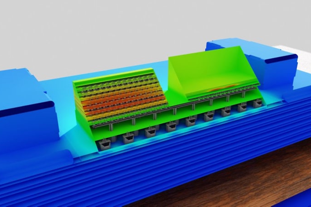
3D-ICs, or multi-die chips, are vertically stacked assemblies of semiconductor chips. A 3D-IC’s compact form factor offers significant performance gains without increasing power consumption. However, denser 3D-ICs complicate design challenges related to electromagnetic issues and the management of heat and stress. It also makes tracing the origins of these problems more difficult. To understand the interactions between 3D-IC components for more advanced applications, 3D multiphysics visualization becomes a requirement for effective design and diagnostics.
Field visualization of 3D-IC with Omniverse
Ansys’ integration of NVIDIA Omniverse, a platform of APIs for developing OpenUSD- and NVIDIA RTX-enabled 3D applications and workflows, will deliver the real-time 3D-IC visualization of results from Ansys solvers, including Ansys HFSS™, Ansys Icepak™, and Ansys RedHawk-SC™. This will help designers interact with 3D models to evaluate critical phenomena like electromagnetic fields and temperature variations. This interactive solution allows designers to optimize next-generation chips to deliver faster data rates, increased functionality, and improved reliability.
“Advanced manufacturing relies on marrying the physical world with the digital,” said Prith Banerjee, chief technology officer at Ansys. “At Ansys, we are harnessing the power of the NVIDIA Omniverse platform to comprehensively simulate and design everything — from tiny semiconductors to the expansive factories where they are produced. Ansys tools, such as RedHawk-SC, already offer visualization features, which are integrated with Omniverse to unlock a new realm of potential”
In addition to integrating Omniverse, RedHawk-SC is now accelerated by NVIDIA Grace CPU Superchips, helping it deliver more performant multiphysics designs.
“Accelerated computing, AI physics, and physically based visualization will drive the next era of industrial digitalization,” said Rev Lebaredian, vice president of Omniverse and simulation technology at NVIDIA. “Ansys semiconductor solutions connected to Omniverse Cloud APIs will help accelerate the electronics ecosystem’s design and engineering processes.”
To see the demonstration of 3D-IC multiphysics visualization with NVIDIA Omniverse, visit Ansys at DAC June 23-27th in San Francisco at booth #1308.


