+44 (0)24 7671 8970
More publications     •     Advertise with us     •     Contact us
 
Loading...
News Article

Adeia selects PulseForge Photonic Debonding equipment

News

Adeia Inc., a leading innovator in research and development who has pioneered hybrid bonding in the semiconductor industry, has chosen PulseForge equipment for advanced heterogeneous integration in semiconductors. The photonic debonding tool was installed at Adeia’s San Jose, CA, facility.

“We are excited to partner with PulseForge and incorporate their state-of-the-art photonic debonding equipment into our advanced packaging facility,” stated Dr. Laura Mirkarimi, senior vice president of engineering at Adeia. “This enhanced capability enables us to process thinned wafers and further drive innovation in the industry.”

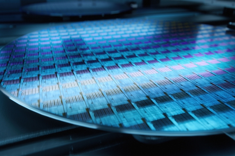
Debonding is a critical process in semiconductor packaging, allowing for the separation of temporarily bonded carriers from thinned wafers. Adeia recognizes the performance of PulseForge’s photonic debonding tool and its unique inorganic light-absorbing layer, which ensures improved yield and a clean debond.

“We are proud to be selected by Adeia as a tool supplier,” said Jonathan Gibson, CEO at PulseForge. “Our photonic debonding technology provides a cost-effective alternative to existing industry methods, and with its unique advantages, we are confident that it will enable Adeia to achieve new levels of performance in their advanced packaging applications.”

The partnership between Adeia and PulseForge underscores the importance of innovation and collaboration in the semiconductor industry. The equipment manufacturer innovations must meet the process technology developer requirements to drive future semiconductor packaging technology advancement

CEA-Leti launches FAMES Pilot Line
Ansys enables 3D multiphysics visualisation of 3D-IC designs
Adeia selects PulseForge Photonic Debonding equipment
Fab capacity predicted to expand six percent in 2024
SEMIFIVE announces commercialisation of its 5nm HPC SoC Platform
Baya Systems to transform and accelerate Intelligent Computing
Computing and AI for automotive: toward centralisation and connectivity
CEA-Leti presents complementary developments in 3D Integration Technologies
Redefining X-ray Beam Monitoring?
Semiconductors in a world without PFAS
QP Technologies expands die preparation business
Advanced Quantum Processing Unit delivered by Pasqal to GENCI and CEA
High-speed, high-temperature pumps address the challenges of advanced ALD processes
Imec introduces 'best-in-class' ADCs
Sparking change in silicon semiconductor manufacturing with green energy
The future of computing runs on silicon-based quantum computing processors
Exploiting the new wave of Semiconductors: AI, trust & information overload
A sustainable semiconductor industry needs smarter water management
The crucial role of ADCs and DACs in scaling quantum computing
Maestro: the AI-infused supply chain orchestration platform
Pfeiffer Vacuum Valves & Engineering receives Blue Sky Award
Silicon’s dual role: Fueling AI’s need for computation and connectivity
Imec demonstrates functional monolithic CFET devices with stacked bottom and top contacts
SEMI focuses on skills initiatives
Sono-Tek to demonstrate SPT200 Photoresist Coating
Microelectronics industry education and workforce challenges explored
PEMTRON to spotlight semiconductor inspection solutions
OMNIVISION introduces 'smallest camera module'
Socionext joins the Global Semiconductor Alliance
Imec unveils CMOS-based 56Gb/s zero-IF D-band beamforming transmitter
Flip chip technology market to reach $45.22 billion in 2032
EV Group and Fraunhofer IZM-ASSID expand partnership
×
Search the news archive

To close this popup you can press escape or click the close icon.
Logo
×
  • 1st January 1970
  • 1st January 1970
  • 1st January 1970
  • 1st January 1970
  • 1st January 1970
  • 1st January 1970
  • 1st January 1970
  • 1st January 1970
  • View all news 22645 more articles
Logo
×
Register - Step 1

You may choose to subscribe to the Silicon Semiconductor Magazine, the Silicon Semiconductor Newsletter, or both. You may also request additional information if required, before submitting your application.


Please subscribe me to:


You chose the industry type of "Other"

Please enter the industry that you work in: