
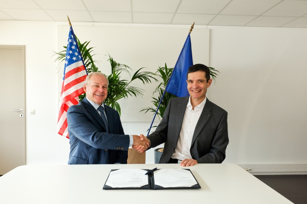
NY CREATES and CEA-Leti form strategic research partnership
NY CREATES and CEA-Leti have announced their strategic partnership that will initially focus on the research and co-development of magnetic memory devices, which are used to store computer data.
These devices would be produced at the 300mm wafer scale, the industry-standard platform upon which computer chips are produced. The announcement was made during the annual Leti Innovation Days in Grenoble.
Officials from the New York Center for Research, Economic Advancement, Technology, Engineering, and Science (NY CREATES), based in Albany, N.Y., USA, and CEA-Leti, based in Grenoble, France, established this joint development agreement to build upon each other’s strengths in the areas related to memory device R&D. CEA-Leti will contribute its expertise in magnetics, spintronics, and the testing of related devices, and NY CREATES will provide the facilities, process integration expertise, and materials process development to run the 300mm silicon hardware.
“By expanding our partnership with CEA-Leti and applying their recognized expertise in device physics and architectures, NY CREATES looks forward to jointly developing innovative technologies for computing. While we are known for our world-class Albany NanoTech Complex with experts in R&D focus areas ranging from advanced logic technologies to heterogeneous integration and more, this initiative’s focus on novel memory is an area in which we can break barriers together,” said NY CREATES President Dave Anderson. “A first objective of this collaboration will be to develop novel magnetic memory architectures and integration. This international partnership will help to address present-day memory needs as computing power continues to progress, and we anticipate a fruitful collaboration.”
“This collaboration will allow CEA-Leti to expand its capability to validate innovative concepts in synergy with the various facilities we have in Grenoble,” said CEA-Leti CEO Sébastien Dauvé. “We strongly believe that our collaboration will be a key enabler for both NY CREATES and CEA-Leti to be much more efficient in the lab-to-fab transition and to better impact our respective local ecosystems with more mature innovations.”
More specifically, the first joint research effort seeks to demonstrate two novel forms of memory devices: Spin Orbit Torque (SOT) Magnetoresistive Random Access Memory (MRAM), and Spin Transfer Torque (STT) MRAM. While both forms of MRAM manipulate different materials’ magnetization to store data, STT MRAM offers non-volatile memory with almost no power leakage; SOT MRAM is considered faster and more efficient.
Leaders of both R&D organizations expect the two-year collaboration to leverage NY CREATES’ 300mm wafer R&D ecosystem centered at its Albany NanoTech Complex, the most advanced non-profit semiconductor R&D facility in North America. CEA-Leti will provide its world-class engineering services and know-how to produce working memory elements on 300mm wafers.


