Loading...
News Article

Ultrafast laser enables new high energy particle strike simulation technique
News

Chromacity Ltd., a technological innovator in the field of ultrafast infrared lasers, has been cited in pioneering research undertaken by Sandia National Laboratories, Albuquerque, USA.

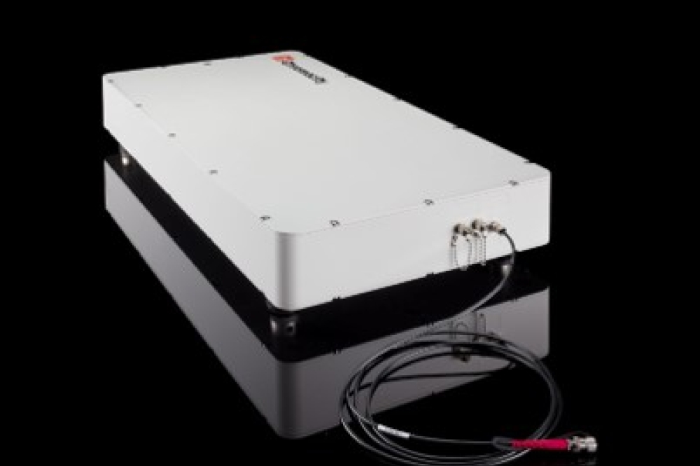
To assess the effectiveness of new semiconductor devices for radiation hardened applications. Sandia used the Chromacity 1280 ultra-fast laser as part of their system to simulate radiation-induced events in logic circuits. High energy particles are known to induce permanent or transitory effects in semiconductor devices. The recent outage in the NASA Voyager 1 spacecraft, where its memory was damaged was likely caused by a high energy particle strike.


Semiconductor devices are becoming more vulnerable to damage caused by high energy particles. Electronics in space have always been vulnerable, with engineers developing an array of countermeasures to mitigate the issues caused by these high energy events. Semiconductor devices are rapidly adopting process technologies with smaller feature sizes, exacerbating the problem, and potentially opening up the possibility of damage in devices used in terrestrial applications.


The Chromacity 1280 has a 1280nm central wavelength and can deliver sub 250fs pulses at a 100MHz repetition rate. It is part of a family of fixed wavelength femtosecond lasers, using the company’s patented hybrid free space and fibre architecture, delivering class leading efficiency in a compact and robust form factor.

Silicon photonics: accelerating growth in the race for high-speed optical interconnects
CCD-in-CMOS technology enables ultra-fast burst mode imaging
2025 6G A look forward
Critical Manufacturing climbs Deloitte’s Technology Fast 50
Semiconductors: The most important thing you probably know the least about
Imec and partners unveil SWIR sensor with lead-free quantum dot photodiodes
Lattice introduces small and mid-range FPGA offerings
SEMI and SMT inspection solutions at NEPCON Japan 2025
Nordic Semiconductor and Kigen demonstrate Remote SIM Provisioning for Massive IoT
Spirent collaborates with Siemens
Quobly forges strategic collaboration with STMicroelectronics
New standards in pressure measurement systems for the semiconductor industry
IBM delivers optics breakthrough
Semiconductor equipment sales to reach $139 Billion in 2026
Marvell introduces 1.6 Tbps LPO Chipset
ACM research strengthens Atomic Layer Deposition portfolio
CEA-Leti demonstrates embedded FeRAM platform compatible with 22nm FD-SOI node
Lattice introduces small and mid-range FPGA offerings
Solace unlocks full potential of event-driven integration
Advantest to showcase latest test solutions at SEMICON Japan 2024
CEA-Leti device integrates light sensing and modulation
Nordic launches Thingy:91 X prototyping platform for cellular IoT and Wi-Fi locationing
Imec achieves seamless InP Chiplet integration on 300mm RF Silicon Interposer
High-precision SMU
Powering India’s energy future
China’s Nvidia probe puts global investors ‘on notice’
POET Technologies appoints new director
Imec demonstrates core building blocks of a scalable, CMOS-fab compatible superconducting digital technology
Imec proposes double-row CFET for the A7 technology node
ULVAC launches new deposition system
Beebolt and SEMI Announce Strategic Partnership to Drive Supplier Resilience and Agility
esmo group introduces Automated Final Test Manipulator
×
Search the news archive

To close this popup you can press escape or click the close icon.
Logo
x
Logo
×
Register - Step 1

You may choose to subscribe to the Silicon Semiconductor Magazine, the Silicon Semiconductor Newsletter, or both. You may also request additional information if required, before submitting your application.


Please subscribe me to:


You chose the industry type of "Other"

Please enter the industry that you work in: