scia Systems highlights advances in ion beam processing
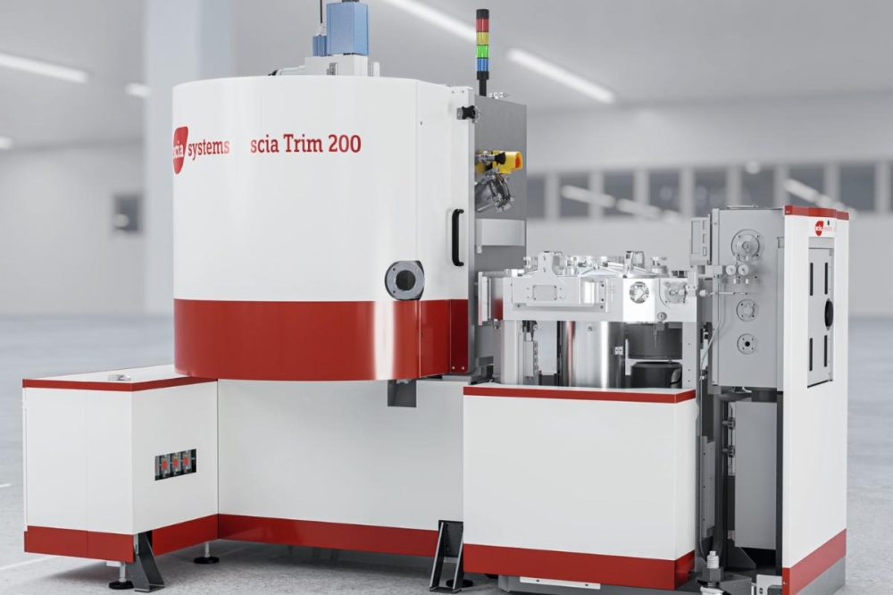
scia Systems’ high-precision ion beam process solutions are enabling the automotive, cloud computing, AR/MR, and mobile communications industries.
scia Systems will highlight key advances in ion beam processing for semiconductor, sensor and photonic integrated circuit (PIC) manufacturing at SEMICON West 2024. The premier microelectronics event will be held July 9-11, 2024, at the Moscone Center in San Francisco, Calif. scia Systems’ high-precision solutions are playing an essential role in enabling many of today’s high-growth consumer and industrial applications.
According to Dr. Michael Zeuner, CEO of scia Systems, “As semiconductors, sensors, and optical devices increase in complexity due to smaller features, new exotic materials, and more layers and complex structures, the processes used to manufacture them require higher levels of precision. Our advances in ultra-precision ion beam process technologies are enabling manufacturers’ success in producing these devices, which are driving cloud computing, augmented/mixed reality (AR/MR), automotive, telecommunications, and many other industries. A case in point, every modern cell phone has components that have been manufactured using a scia Systems product. We look forward to highlighting these solutions, as well as the many high-growth applications that they enable, at SEMICON West – the premier event for the semiconductor ecosystem.”
Demand for PICs is growing rapidly in telecommunications and data centers due to their wide bandwidth, low transmission loss, and numerous other advantages over traditional electronic integrated circuits. Integrating new materials, material stacks, and designs requires new etching solutions. scia Systems’ advanced ion beam etching and trimming processes enable manufacturing of three-dimensional optoelectronic microstructures for PICs, such as waveguides and other optical components. Reducing microroughness by ion beam trimming is another promising application area that enhances the production of high-performance PICs. Further applications include nano-structured surface relief gratings for AR/MR systems, and surface form error correction for telescope mirrors, X-ray optics, lenses, and conventional optics.
High-precision sensors that use magnetic storage, most notably giant magnetoresistance (GMR) and tunnel magnetoresistance (TMR) sensors, are used to detect any type of motion including proximity, rotations or vibrations. These have been rapidly adopted across a wide variety of industries and applications, including automotive electronics, industrial equipment, and cloud storage. However, the complex, multi-layer composition of these sensors creates significant challenges for traditional chemical and dry etching processes, which have difficulty processing magnetic materials. scia Systems overcomes these limitations with its high-precision ion beam etching technology, enabling the manufacture of high-performance GMR sensors for flexible and wearable electronics, including AR/MR headsets, and TMR sensors for Internet of Things (IoT), automotive, smart home, eMobility, and many other applications.
Reverse engineering is an essential step in semiconductor manufacturing. By conducting verification, failure analysis, and research of internal device structures, engineers can isolate and troubleshoot problems to improve manufacturing yields. Reverse engineering involves exposing internal components, delayering to analyze each layer of the device, imaging, and post-processing. Conventional delayering processes such as wet chemical etching, CMP or plasma etching are often expensive, error-prone, and limited in application. scia Systems’ ion beam etching technology enables precise processing within the micro- and nanometer-size range and atomic-level-thickness range for different materials at once.


