Resonac unveils new US-JOINT Consortium

The consortium will help to further advance technology in back-end packaging, an area that has not been significantly focused on in the US.
Resonac has unveiled a new consortium of ten partners, called “US-JOINT,” for its semiconductor back-end process R&D in Silicon Valley. The ten American and Japanese semiconductor materials and equipment companies are: Azimuth; KLA; Kulicke & Soffa; Moses Lake Industries; MEC; ULVAC; NAMICS; TOK; TOWA; and Resonac.
US-JOINT expands the activities of Japan-based open consortiums led by Resonac (known as "JOINT" and "JOINT2") in the U.S. and includes the participation of five U.S.-based companies. US-JOINT R&D will take place at a new R&D center in Union City, Calif., set up through co-investment with the partners. The construction of cleanrooms and equipment installation will begin this year, and the facility is expected to be fully operational in 2025.
Mr. Rahm Emanuel, the U.S. Ambassador to Japan, said, “With nearly every area of our daily lives now dependent on semiconductors, it is critical that we strengthen supply chains through cooperation with trusted partners in the sector. This new consortium of leading American and Japanese companies in the semiconductor industry is the latest example of our two nations joining forces to accelerate the development of advanced technologies of global importance.”
US-JOINT is an open consortium designed for end-customer collaboration to verify the latest requirements for semiconductor packaging of advanced devices and validate new concepts in development. In addition, by co-creating with customers, Resonac and the US-JOINT members will capture market needs in real time, accelerating the R&D of materials and equipment technologies.
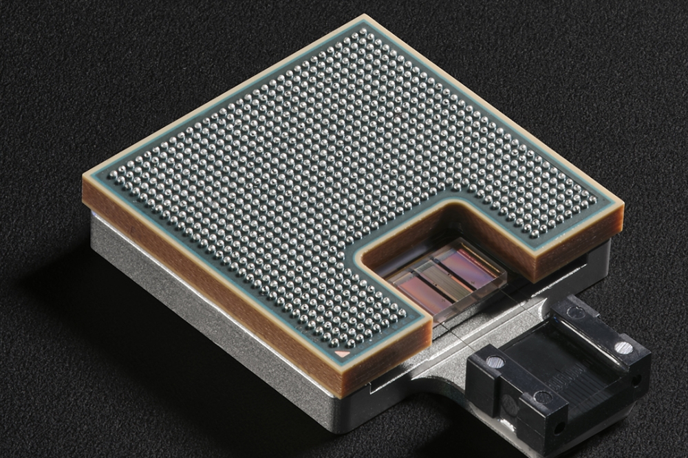
“Today’s rapidly expanding next-generation semiconductors for generative AI and autonomous driving require new approaches to advanced packaging technologies, such as 2.5D and 3D1,” said Hidenori Abe, executive director of Electronics Business Headquarters, Resonac. “In recent years, major semiconductor manufacturers and fabless companies in Silicon Valley, including GAFAM2, are designing semiconductors in-house and creating new concepts in back-end packaging one after another. This is where the US-JOINT consortium can contribute significantly with our leading technology in materials and equipment on-shore in the U.S.”
Advanced packaging and back-end processing of semiconductors has traditionally been located primarily in Asia. Bringing packaging R&D closer to major semiconductor device makers in Silicon Valley will help to further advance the technology and solve technical issues, especially in the areas that other U.S. consortiums do not cover enough, including advancements in the substrate, interposer and fabrication of the package.
Jan Vardaman, president, TechSearch International, Inc., said, "This represents a tremendous opportunity for U.S. companies to take advantage of the expertise gathered in material and equipment for advanced packaging development."


