
ISE Labs expands capabilities, doubles lab space
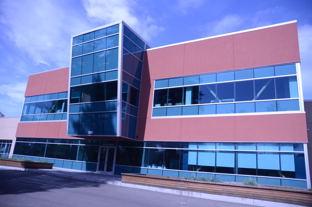
ISE Labs, a leading provider of semiconductor engineering services, is broadening customer access to its world-class capabilities with the opening of a second U.S. facility, located in San Jose, Calif.
Together, the Fremont and San Jose sites will double the available R&D lab space to 100,000 square feet, reinforcing the company’s commitment to Silicon Valley while expanding its North American footprint and helping to strengthen the U.S. semiconductor supply chain.
ISE Labs purchased the building in late 2023 and has built it out specifically to accommodate the engineering needs of its North American customers, many of whom are working on solutions for emerging semiconductor applications, such as artificial intelligence/machine learning (AI/ML), advanced driver assistance systems (ADAS), and high-performance computing (HPC), to name a few. In addition to shifting some team members between facilities, ISE Labs is seeking a small number of highly skilled engineers and technicians for the new site.
According to Kenneth Hsiang, Chief Executive Officer, ISE Labs, “As semiconductor manufacturing supply chain reshoring continues to escalate, demand for our proven engineering expertise is growing in parallel. Expanding our operations by adding a second facility is vital to support our growing customers, who are onsite daily due to the collaborative nature of our work. Ease of access in the South Bay was a key consideration in selecting our new site.”
The San Jose facility will primarily house qualification and reliability process, including environmental, mechanical, electrostatic discharge (ESD), failure analysis, and burn-in. ISE Labs’ high-power burn-in solutions – vital to detecting early failures in a semiconductor device – are among the best and highest-performing in the industry. The Fremont site will expand its already robust set of test functions, including automated test equipment (ATE) test program development, test hardware design, device characterization, wafer probing, and engineering, pre-production and final test, and system-level test.
“We are firmly committed to our investment in Silicon Valley. It both contributes to the region’s revitalizing its position in the semiconductor industry and supports U.S. manufacturers more broadly. Adding this new high-end facility to our existing local footprint is an important step,” said Dr. Tien Wu, Chief Executive Officer, ASE, Inc. “Our ISE Labs division – the largest semiconductor testing service provider in North America – is essential to advancing ASE’s role in driving the development of the world’s most innovative electronics.”
Jui Ko, President, ISE Labs, and Dr. Tien Wu, CEO, ASE Group, will preside over the grand opening event, which will feature remarks from San Jose Mayor Matt Mahan; Poonum Patel, Deputy Director of Business Development, Governor’s Office of Business and Economic Development (GO-Biz); and other dignitaries, followed by a ribbon-cutting. The agenda will then segue into two brief, dynamic Q&A panel sessions that will further underscore the significance of the new facility to the companies, the region, and the semiconductor industry supply chain. A networking luncheon and facility tours will complete the event.


