Loading...
News Article

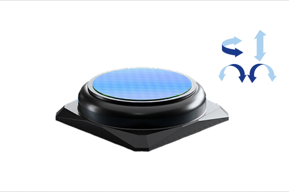
Highly dynamic 4DOF Piezo Wafer Stage for inspection and metrology

News

Leveraging decades of piezo nanopositioning technology experience, introducing at 2024 Semicon West.

PI’s newest wafer inspection solution is based on a hybrid kinematics design, combining Piezo-Walk motors and piezo stacks to achieve both long travel and highly dynamic, ultra-precise motion. This integrated 4-DOF solution reduces equipment complexity, integration efforts, costs, and risks.

Piezo-Walk motors are self-locking at rest, adding no servo dither and heat, unlike other motion techniques. The high bandwidth of the short-travel piezo stack actuators allows for dynamic tracking and error compensation of external disturbances (e.g., from long travel XY wafer stages).

The 4DOF module can also correct for rotational wafer misalignment and takes wafer thickness and machine static characteristics into account.

The high-stiffness design of the Tip-Tilt drive module provides extremely fast step and settle (<10msec) and position stability (<0.05µrad).

Silicon photonics: accelerating growth in the race for high-speed optical interconnects
CCD-in-CMOS technology enables ultra-fast burst mode imaging
2025 6G A look forward
Critical Manufacturing climbs Deloitte’s Technology Fast 50
Semiconductors: The most important thing you probably know the least about
Imec and partners unveil SWIR sensor with lead-free quantum dot photodiodes
Lattice introduces small and mid-range FPGA offerings
SEMI and SMT inspection solutions at NEPCON Japan 2025
Nordic Semiconductor and Kigen demonstrate Remote SIM Provisioning for Massive IoT
Spirent collaborates with Siemens
Quobly forges strategic collaboration with STMicroelectronics
New standards in pressure measurement systems for the semiconductor industry
IBM delivers optics breakthrough
Semiconductor equipment sales to reach $139 Billion in 2026
Marvell introduces 1.6 Tbps LPO Chipset
ACM research strengthens Atomic Layer Deposition portfolio
CEA-Leti demonstrates embedded FeRAM platform compatible with 22nm FD-SOI node
Lattice introduces small and mid-range FPGA offerings
Solace unlocks full potential of event-driven integration
Advantest to showcase latest test solutions at SEMICON Japan 2024
CEA-Leti device integrates light sensing and modulation
Nordic launches Thingy:91 X prototyping platform for cellular IoT and Wi-Fi locationing
Imec achieves seamless InP Chiplet integration on 300mm RF Silicon Interposer
High-precision SMU
Powering India’s energy future
China’s Nvidia probe puts global investors ‘on notice’
POET Technologies appoints new director
Imec demonstrates core building blocks of a scalable, CMOS-fab compatible superconducting digital technology
Imec proposes double-row CFET for the A7 technology node
ULVAC launches new deposition system
Beebolt and SEMI Announce Strategic Partnership to Drive Supplier Resilience and Agility
esmo group introduces Automated Final Test Manipulator
×
Search the news archive

To close this popup you can press escape or click the close icon.
Logo
x
Logo
×
Register - Step 1

You may choose to subscribe to the Silicon Semiconductor Magazine, the Silicon Semiconductor Newsletter, or both. You may also request additional information if required, before submitting your application.


Please subscribe me to:


You chose the industry type of "Other"

Please enter the industry that you work in: