
SkyWater invests in MEBL
Positions SkyWater’s Minnesota fab with the most advanced 200 mm lithography offering in the world.
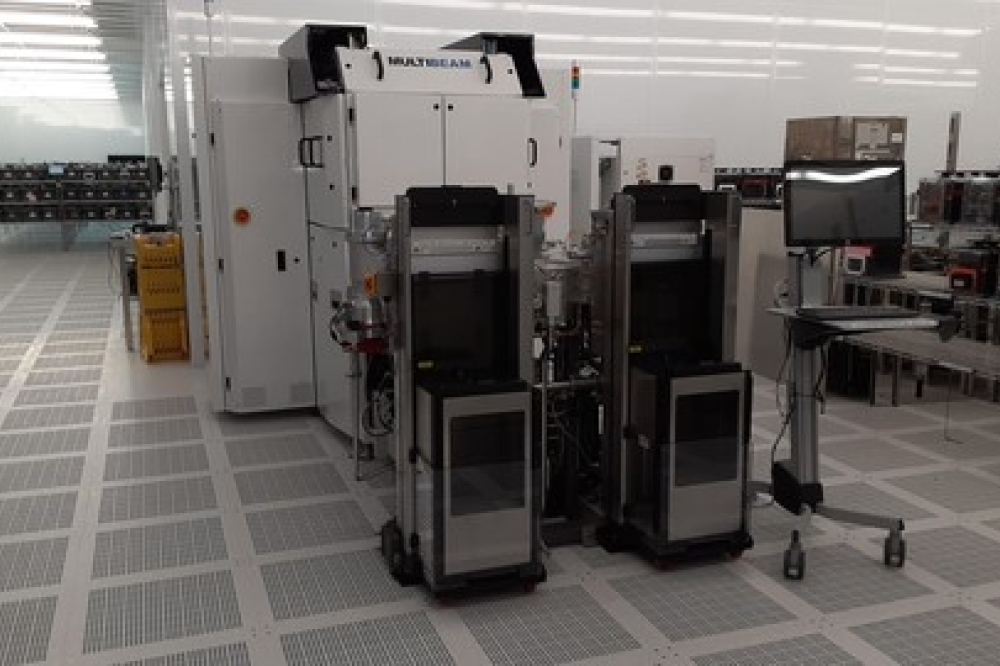
SkyWater Technology has received from Multibeam Corp., a first-of-a-kind Multicolumn E-Beam Lithography (MEBL) system for volume production. The Multibeam (MB) platform is a landmark for the semiconductor industry, offering a high-throughput direct write patterning system that is orders of magnitude faster and more productive than conventional e-beam tools. The MB system will be available to SkyWater customers for early concept prototyping and rapid production.
“We are excited to offer new lithography capabilities to our customers enabled by Multibeam’s revolutionary technology. The deployment of the MB platform will expand capabilities and time to market for innovators on the concept-to-production journey in secure defense, biomedical, thermal imaging, high reliability and advanced compute markets.”
MEBL enables several new production capabilities for SkyWater’s customers including secure chip ID for anti-counterfeit applications and full wafer patterning to support focal plane read-out ICs and other types of large format die. MEBL also offers large depth of focus for a range of high topology microfluidic and MEMS architectures, curvilinear designs for photonics, and high-density MOS. In addition, it is the only production lithography tool capable of sub 50 nm geometries on 200 mm wafers.
Uniquely configured with multiple miniaturized electron beam columns, the MB platform elevates E-Beam Lithography (EBL) to a breakthrough maskless lithography production system with compelling performance and cost advantages for today’s IC fabs. The delivery of the first Multibeam system follows a close collaboration with SkyWater over the past two years. This partnership provided critical fab operational insights which were used to define key system performance specifications before delivery of the MB platform to SkyWater.
According to Multibeam Chairman and CEO, Dr. David K. Lam, “This is a significant milestone for Multibeam and we are immensely proud to share it with SkyWater. From the outset of our engagement with SkyWater they supported our mission to re-innovate EBL for high-volume production and provided critical user perspectives that helped us accelerate our development program and commercialize a world-class maskless lithography system. We are grateful for their collaboration and thrilled to place our first production tool in a SkyWater fab.”
SkyWater CEO and Director, Thomas Sonderman emphasized the value of this technology for customers across target growth markets, “We are excited to offer new lithography capabilities to our customers enabled by Multibeam’s revolutionary technology. The deployment of the MB platform will expand capabilities and time to market for innovators on the concept-to-production journey in secure defense, biomedical, thermal imaging, high reliability and advanced compute markets.”
Sonderman added: “Our engagement with Multibeam exemplifies the power of partnerships in developing breakthrough equipment to accelerate chip innovation in the U.S. and positions SkyWater’s Minnesota fab with the most advanced 200 mm lithography in the world.”
SkyWater will enable access to the tool for initial customer designs in 4Q24.


