
ACM Research enters Fan-out Panel Level Packaging market
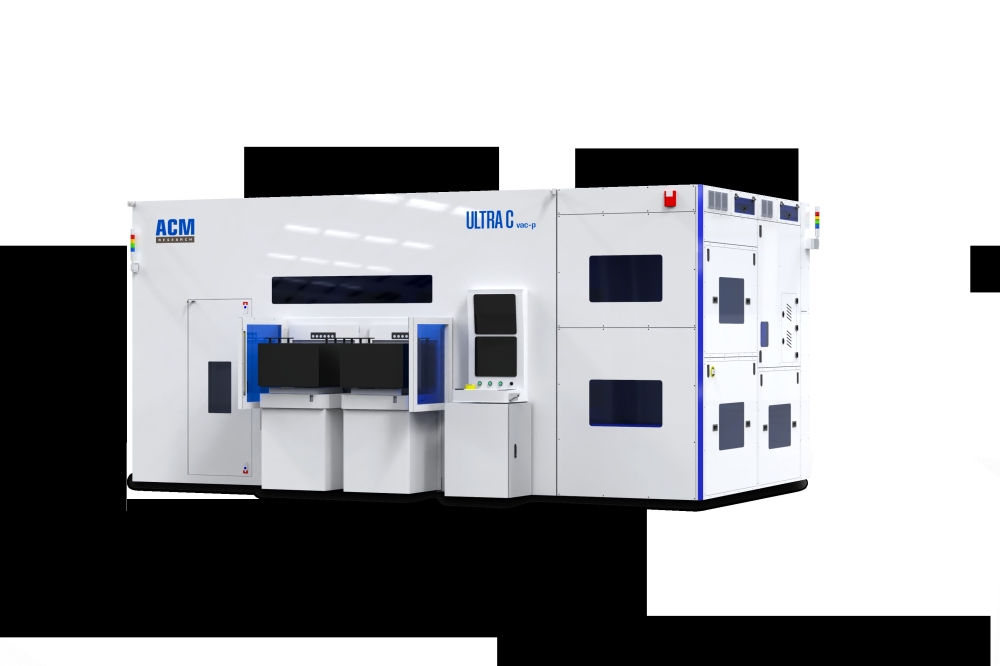
Ultra C vac-p Flux Cleaning Tool for chiplets uses vacuum technology and IPA drying to enhance cleaning efficiency enabling cost-effective semiconductor advanced packaging.
ACM Research has introduced the Ultra C vac-p flux cleaning tool for fan-out panel-level packaging (FOPLP). Utilizing vacuum technology, the new tool efficiently removes flux residues from chiplet structures. ACM also announced today it received a purchase order from a major China semiconductor manufacturer which has been shipped to the customer’s facility in July.
“The demand for greater computing power, lower latency and higher bandwidth driven by AI, data centers and autonomous vehicles makes FOPLP an increasingly essential technology,” said Dr. David Wang, ACM’s President and Chief Executive Officer. “FOPLP integrates multiple chips, passive components and interconnections within a single panel-packaged unit, enhancing flexibility, scalability and cost-efficiency. ACM’s Ultra C vac-p represents a major advancement in addressing the cleaning challenges associated with next-generation advanced packaging technologies. This launch not only underscores ACM’s ongoing innovation in semiconductor manufacturing, but also our commitment to address the evolving needs of the industry."
According to Yole Group, FOPLP adoption will grow faster than the overall fan-out market, and its market share will move from 2% in 2022 to 8% in 2028. The growth of FOPLP is primarily driven by its potential cost savings. For instance, panels typically utilize more than 95% of the material due to their rectangular or square shape, whereas traditional silicon wafers use less than 85% of the material due to their circular shape. The effective area of a 600x600mm panel is also 5.7 times larger than that of a traditional 300mm silicon wafer, enabling overall cost reductions of approximately 66%. This enhanced area utilization leads to higher throughput, greater AI chip design flexibility, and significant cost savings.
The Ultra C vac-p tool addresses critical steps in the advanced packaging process, particularly the removal of flux residue before underfilling, which is essential for eliminating voids. Traditional cleaning methods often fail with small bump pitches (less than 40 microns) and large chip sizes due to surface tension and limited liquid penetration. The vacuum technology in ACM’s new tool ensures the cleaning liquid thoroughly reaches all gaps, even in large panel substrates where traditional methods fall short. Combined with ACM’s proprietary IPA drying technology, this comprehensive cleaning process prevents residues that could impair device performance.
About the Ultra C vac-p Cleaning Tool
The Ultra C vac-p Cleaning tool is designed for panel substrates and accommodates both organic and glass materials. It is capable of handling panels sized 510 mm x 515 mm and 600 mm x 600 mm, while effectively managing cover warpages up to 7mm.


