+44 (0)24 7671 8970
More publications     •     Advertise with us     •     Contact us
 
Loading...
News Article

ACM Research strengthens its fan-out panel level packaging portfolio

News

Launch of Ultra ECP ap-p Tool - delivering superior uniformity, enabling performance and cost efficiencies for next generation chip packaging.

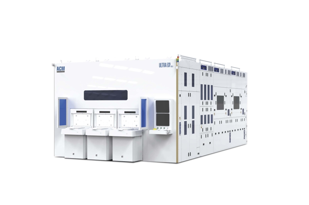
ACM Research has introduced its new Panel Electrochemical Plating (Ultra ECP ap-p) tool designed for fan-out panel-level packaging (FOPLP). This new tool employs a horizontal plating approach achieving superior uniformity and precision across the entire panel.

“As demands for low latency, high bandwidth and cost-efficiency in semiconductor chips intensify, advanced packaging technologies like FOPLP are becoming increasingly critical,” said Dr. David Wang, ACM’s President and Chief Executive Officer. “FOPLP, with its capability to facilitate high-density, high bandwidth chip-to-chip connections, offers substantial growth prospects. The Ultra ECP ap-p tool is the first in the world to employ horizontal plating for panel applications, drawing upon ACM’s deep-rooted expertise in wafer plating and copper processes. We believe the tool will revolutionize the market, enabling advanced packaging with sub-micron features on large panels, which are especially applicable to GPUs and high-density high bandwidth memory (HBM).”

The Ultra ECP ap-p tool supports 515mm x 510mm panel sizes, with an option to expand to 600mm x 600mm. It is compatible with both organic and glass substrates and includes capabilities for copper (Cu) via filling, Cu pillar, nickel (Ni), tin-silver (SnAg) plating, and solder bumping. It accommodates high-density fan-out (HDFO) products requiring Cu, Ni, SnAg and gold plating.

ACM’s proprietary technology optimizes the management of electrical fields, ensuring consistent and uniform plating across the panel. The horizontal configuration of the tool significantly reduces the risk of cross-contamination between baths, enhancing control and cleanliness, crucial for producing large panels with sub-micron redistribution layers (RDLs) and micro-pillars.

The Ultra ECP ap-p tool incorporates advanced automation features that enhance efficiency and quality control throughout the manufacturing process. This automation not only mirrors traditional wafer processing steps. but also adapts them for larger and heavier panels, including critical operations like panel flipping for correct orientation and face-down plating.

Exyte selects LTIMindtree
TRI to display new Wafer Inspection and Metrology solution
Advanced CMOS design sets 'new benchmark' in ultra-fast sensors
Industry to address child care needs
EU project ARCTIC joins quantum forces
Advantest celebrates 25th anniversary of V93000 SoC Test Platform
Advanced packaging in Europe: Swissbit hosts EuroPAT Workshop 2024
Introducing the N-332 - Vacuum Compatible Nanopositioning Stage family
ACM Research strengthens its fan-out panel level packaging portfolio
Imec demonstrates logic and DRAM structures using High NA EUV Lithography
Yongjiang Laboratory orders Reactive Ion Beam Trimming equipment from scia Systems
Paving the way for the semiconductor future
Government scheme helps UK chip start-ups raise £10 million
Renesas completes acquisition of Altium
Greene Tweed highlights Chemraz 541
Intel acts to 'accelerate progress'
Infineon reports slight increase in revenue and earnings in Q3 FY 2024
New partnership brings semiconductor manufacturing to Central Valley
Merck joins German research project "Semiconductor-X"
V-Nova and Amlogic form partnership
AMI joins NXP Semiconductors Partner Program
EFC Gases & Advanced Materials announces $210 million investment
Promex Industries and QP Technologies implement sales/marketing reorganisation
Amkor signs preliminary Memorandum of Terms with US Department of Commerce
Ansys 2024 R2 delivers multiphysics innovation
Infineon introduces Edge AI evaluation kit
Nearfield Instruments to supply QUADRA Metrology System to Asian fab
ACM Research enters Fan-out Panel Level Packaging market
Nanotronics unveils nSpec ES
Samsung Electro-Mechanics collaborates with AMD
3D-Micromac receives laser-trimming system order from Infineon
Agile Analog delivers customisable IP on GlobalFoundries’ FinFet and FDX processes
×
Search the news archive

To close this popup you can press escape or click the close icon.
Logo
×
  • 1st January 1970
  • 1st January 1970
  • 1st January 1970
  • 1st January 1970
  • 1st January 1970
  • 1st January 1970
  • 1st January 1970
  • 1st January 1970
  • View all news 22645 more articles
Logo
×
Register - Step 1

You may choose to subscribe to the Silicon Semiconductor Magazine, the Silicon Semiconductor Newsletter, or both. You may also request additional information if required, before submitting your application.


Please subscribe me to:


You chose the industry type of "Other"

Please enter the industry that you work in: