+44 (0)24 7671 8970
More publications     •     Advertise with us     •     Contact us
 
Loading...
News Article

Advanced CMOS design sets 'new benchmark' in ultra-fast sensors

News

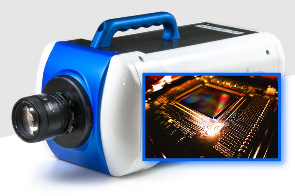
SI Sensors design novel CMOS image sensors for ultra-fast cameras that increase the velocity of the signal electrons allowing them to be swept out of the photodiode and be detected much faster.

Developing ultra-high-speed CMOS image sensors is difficult because at very high frame rates, the integration time is extremely short and there is never enough light. Consequently, these ultra-high speed image sensors require very high sensitivity (Quantum Efficiency) such that no photons are wasted.

General Manager of SI Sensors - Philip Brown commented “Detecting weak signals is all about maximising the signal to noise ratio. It is therefore equally important to minimise noise sources within the sensor such that the relatively weak signal provided by the limited available light can be detected above the noise floor. However, running the various sampling circuits within an image sensor at high speed tends to increase the noise. The design of these circuits including the individual transistor geometries and layout must be optimised with regards to speed and noise, which requires intimate knowledge of the mixed signal circuit design and fabrication processes used, as well as significant simulation and verification using cutting edge software design tools. Drawing upon our team of highly experienced CMOS specialists - SI Sensors are designing image sensors which are approaching the limit of what is physically possible. For ultra-fast imaging we have designed novel structures within the photodiode to create drift fields which increase the velocity of the signal electrons to allow them to be swept out of the photodiode to be detected much faster”.

He added “SI Sensors are developing innovative ultra-fast image sensors that will find application in the next generation of ultra high-speed cameras. Using our next generation CMOS sensor technology these cameras will enable scientists and engineers to image ultra-fast phenomena more precisely, and in more detail than ever before and help progress developments in applications including nuclear fusion, ballistics, detonics, medical research, spray analysis, combustion research, nanotechnology and failure dynamics”.

Exyte selects LTIMindtree
TRI to display new Wafer Inspection and Metrology solution
Advanced CMOS design sets 'new benchmark' in ultra-fast sensors
Industry to address child care needs
EU project ARCTIC joins quantum forces
Advantest celebrates 25th anniversary of V93000 SoC Test Platform
Advanced packaging in Europe: Swissbit hosts EuroPAT Workshop 2024
Introducing the N-332 - Vacuum Compatible Nanopositioning Stage family
ACM Research strengthens its fan-out panel level packaging portfolio
Imec demonstrates logic and DRAM structures using High NA EUV Lithography
Yongjiang Laboratory orders Reactive Ion Beam Trimming equipment from scia Systems
Paving the way for the semiconductor future
Government scheme helps UK chip start-ups raise £10 million
Renesas completes acquisition of Altium
Greene Tweed highlights Chemraz 541
Intel acts to 'accelerate progress'
Infineon reports slight increase in revenue and earnings in Q3 FY 2024
New partnership brings semiconductor manufacturing to Central Valley
Merck joins German research project "Semiconductor-X"
V-Nova and Amlogic form partnership
AMI joins NXP Semiconductors Partner Program
EFC Gases & Advanced Materials announces $210 million investment
Promex Industries and QP Technologies implement sales/marketing reorganisation
Amkor signs preliminary Memorandum of Terms with US Department of Commerce
Ansys 2024 R2 delivers multiphysics innovation
Infineon introduces Edge AI evaluation kit
Nearfield Instruments to supply QUADRA Metrology System to Asian fab
ACM Research enters Fan-out Panel Level Packaging market
Nanotronics unveils nSpec ES
Samsung Electro-Mechanics collaborates with AMD
3D-Micromac receives laser-trimming system order from Infineon
Agile Analog delivers customisable IP on GlobalFoundries’ FinFet and FDX processes
×
Search the news archive

To close this popup you can press escape or click the close icon.
Logo
×
  • 1st January 1970
  • 1st January 1970
  • 1st January 1970
  • 1st January 1970
  • 1st January 1970
  • 1st January 1970
  • 1st January 1970
  • 1st January 1970
  • View all news 22645 more articles
Logo
×
Register - Step 1

You may choose to subscribe to the Silicon Semiconductor Magazine, the Silicon Semiconductor Newsletter, or both. You may also request additional information if required, before submitting your application.


Please subscribe me to:


You chose the industry type of "Other"

Please enter the industry that you work in: